3 ac characteristics, 1 basic bus cycle, Tmp92cz26a – Toshiba H1 Series User Manual
Page 648: Output level: high = 0.7 3av, Low = 0.3 3av, Input level: high = 0.9 3av, Low = 0.1 3av
TMP92CZ26A
92CZ26A-645
4.3 AC
Characteristics
The Following all AC regulation is the measurement result in following condition, if unless otherwise noted.
AC measuring condition
•
Clock of top column in above table shows system clock frequency, and “T” shows system
clock period [ns].
•
Output level: High
= 0.7 3AV
CC
, Low
= 0.3 3AV
CC
•
Input level: High
= 0.9 3AV
CC
, Low
= 0.1 3AV
CC
Note: In table, “Variable” shows the regulation at DVCC3A=3.0V~3.6V, DVCC1A=DVCC1B=DVCC1C=1.4~1.6V.
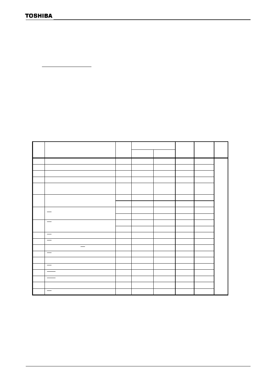
4.3.1
Basic Bus Cycle
Read cycle
Variable
No. Parameter Symbol
Min Max
80 MHz 60 MHz Unit
1 OSC period (X1/X2)
t
OSC
100 166.6
−
−
2 System clock period (
= T)
t
CYC
12.5 266.6 12.5 16.6
3 SDCLK
low
width
t
CL
0.5T
− 3
3.25
5.3
4 SDCLK
high
width
t
CH
0.5T
− 3
3.25
5.3
5-1
A0 ~ A23 valid
→ D0 ~ D15 input at 0
waits
t
AD
2.0T
− 18.0
7
15.3
t
AD6
6.0T
− 18.0
−
82
5-2
A0 ~ A23 valid
→ D0 ~ D15 input at
4 waits
/6 waits
t
AD7
8.0T - 18.0
82
−
t
RD
1.5T
− 18.0
−
7
6-1
RD
falling
→ D0 ~ D15 input at 0 waits
t
RD
1.5T
− 18.0
0.75
−
t
RD6
5.5T
− 18.0
−
73.6
6-2
RD
falling
→ D0 ~ D15 input at
4 waits
/6waits
t
RD7
5.5T
− 18.0
50.75
−
7-1
RD
low width at 0 waits
t
RR
1.5T
− 10
8.75
14.9
7-2
RD
low width at
4 waits
t
RR6
5.5T
− 10
58.75
81.3
8 A0 ~ A23 valid →
RD
falling
t
AR
0.5T
− 5
1.25
3.3
9
RD
falling
→ SDCLK rising
t
RK
0.5T
− 5
1.25
3.3
10 A0 ~ A23 valid
→ D0 ~ D15 hold
t
HA
0 0
0
11
RD
rising
→ D0 ~ D15 hold
t
HR
0 0
0
12
WAIT
setup time
t
TK
3 3
5
13
WAIT
hold time
t
KT
2
2 3
14 Data byte control access time
t
SBA
1.5T
− 18.0
0.75
7
15
RD
high width
t
RRH
0.5T
− 5
1.25
3.3
ns
AC measuring condition
• Data_bus, Address_bus, various function control signal capacitance C
L
= 50 pF
Note: The operation guarantee temprature: 80MHz: Ta=0
∼50°C
,
less than 60MHz: Ta=0
∼70°C