2 touch screen interface (tsi) control register – Toshiba H1 Series User Manual
Page 568
TMP92CZ26A
92CZ26A-565
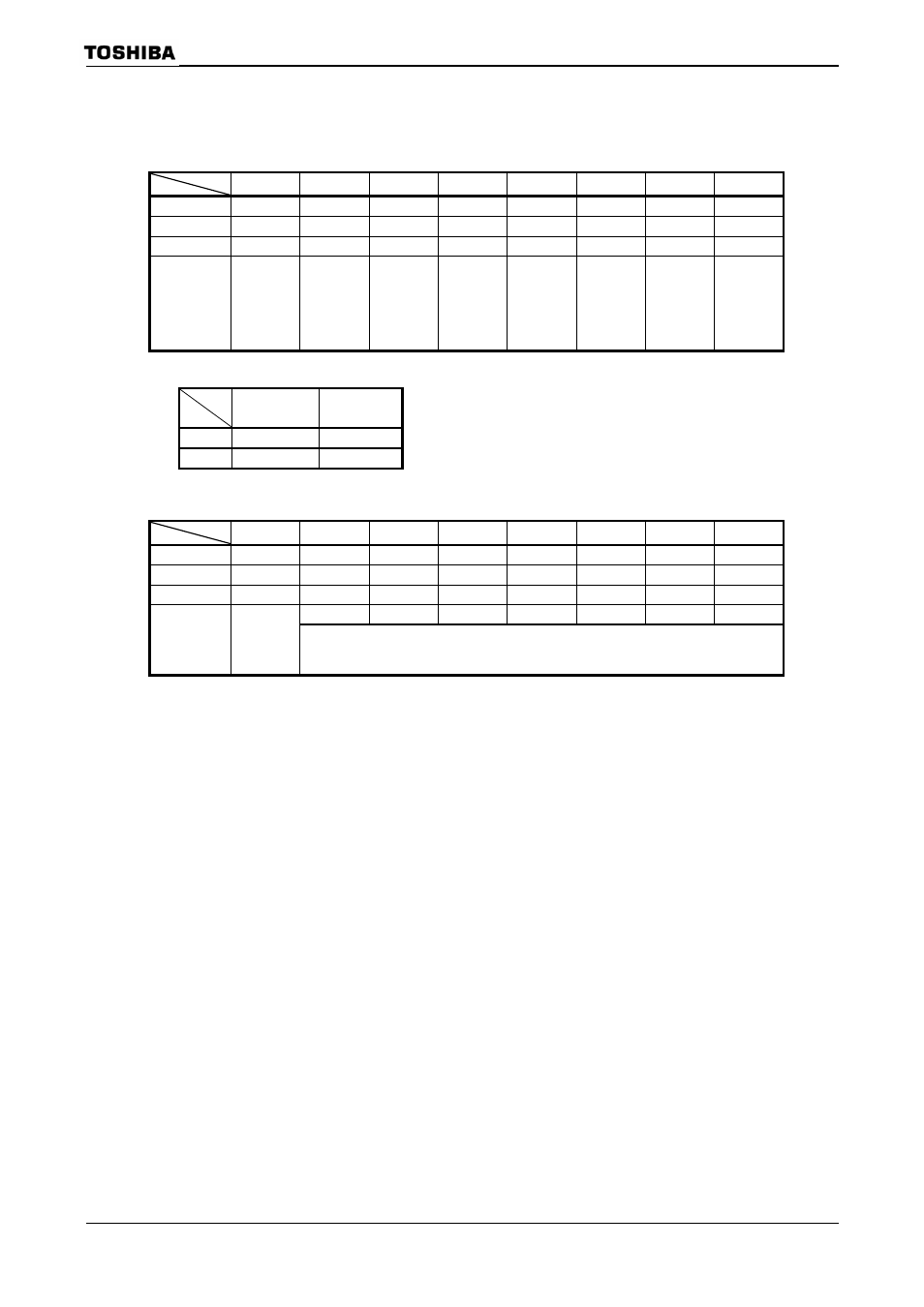
3.20.2 Touch Screen Interface (TSI) Control Register
TSI control register
7 6 5 4 3 2 1 0
bit
Symbol TSI7 INGE PTST TWIEN PYEN PXEN MYEN MXEN
Read/Write
R/W R/W R R/W R/W R/W R/W R/W
After
reset
0 0 0 0 0 0 0 0
Function
0: Disable
1: Enable
Input gate
control of
Port 96,97
0: Enable
1: Disable
Detection
condition
0: no
touch
1: touch
INT4
interrupt
control
0: Disable
1: Enable
SPY
0 : OFF
1 : ON
SPX
0 : OFF
1 : ON
SMY
0 : OFF
1 : ON
SMX
0 : OFF
1 : ON
De-bounce time setting register
7 6 5 4 3 2 1 0
bit
Symbol
DBC7
DB1024
DB256
DB64 DB8 DB4 DB2 DB1
Read/Write
R/W R/W R/W R/W R/W R/W R/W R/W
After
reset
0 0 0 0 0 0 0 0
1024
256
64 8 4 2 1
Function
0: Disable
1: Enable
De-bounce time is set by “(N*64-16) / f
SYS
”-formula.
“N” is sum of number which is set to “1” in bit6 to bit 0. Note3:
Note1: Since an internal clock is used for de-bounce circuit, when IDLE1, STOP mode or PCM condition, the de-bounce
circuit don’t operate and also interrupt which through this circuit is not generated. When IDLE1, STOP mode or PCM
condition, set this circuit to disable (Write “0” to TSICR1
to “0”, signal is received after counting the 6-system clock (f
SYS
) from the condition that this circuit is set to disable.
Note2: During converting the analog input-data by using AD converter, the current flow to the normal C-MOS input-gate.
Therefore, provide its current by setting TSICR0
C-MOS logic (P96,P97) by settig this bit.
Note3: TSICR0
TSICR0
Ex:
TSICR1=95H
→N = 64 + 4 + 1 = 69
TSICR0
(01F0H)
<
PXEN
>
0 1
0
OFF OFF
1
ON OFF
PXD (internal pull-down resistor) ON/OFF setting
TSICR1
(01F1H)