Tmp92cz26a – Toshiba H1 Series User Manual
Page 279
TMP92CZ26A
92CZ26A-276
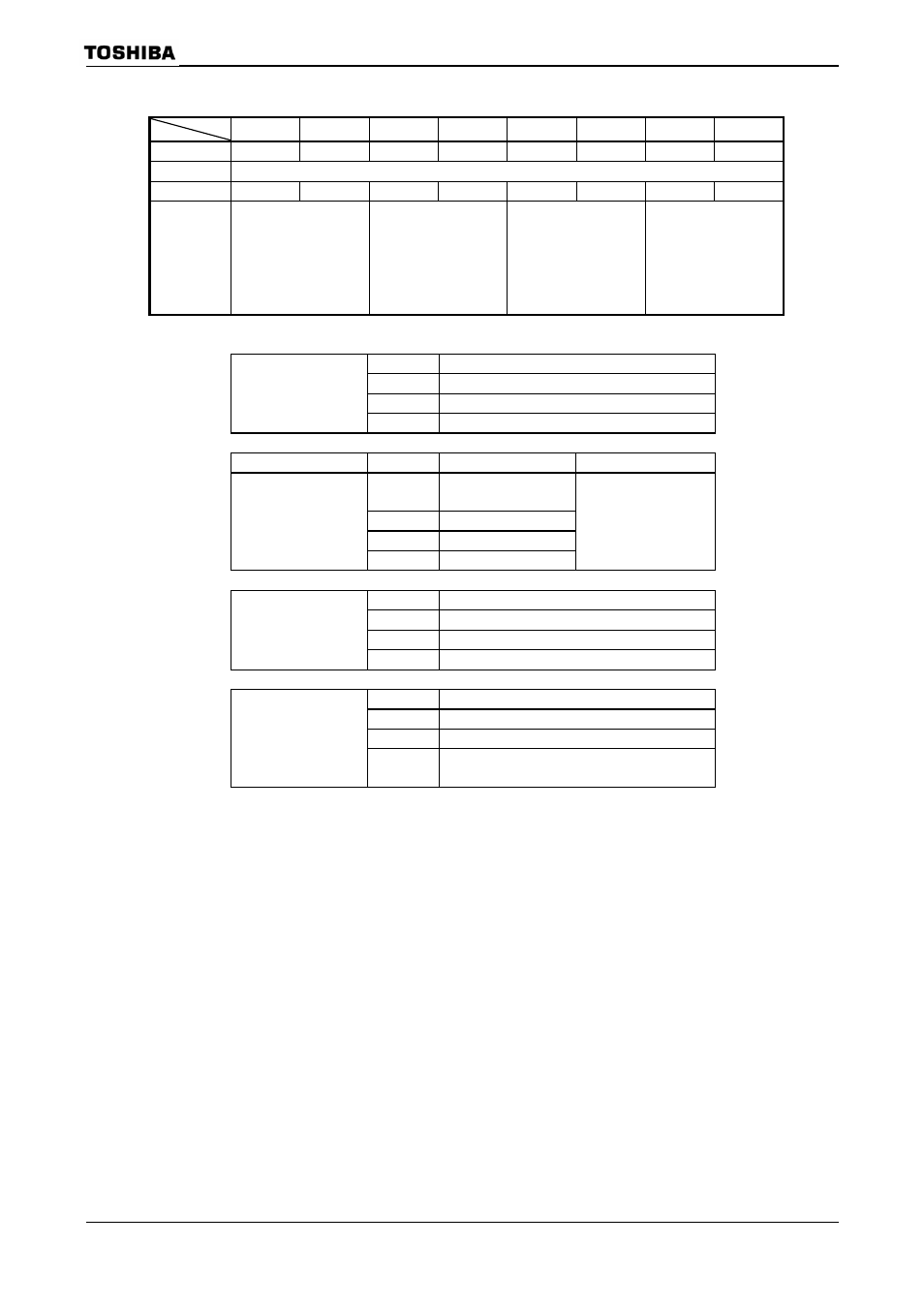
TMRA01 Mode Register
7 6 5 4 3 2 1 0
Bit symbol
TA01M1
TA01M0
PWM01
PWM00
TA1CLK1
TA1CLK0
TA0CLK1 TA0CLK0
Read/Write R/W
After
reset
0 0 0 0 0 0 0 0
Function Operation
mode
00: 8-bit timer mode
01: 16-bit timer mode
10: 8-bit PPG mode
11: 8-bit PWM mode
PWM cycle
00: Reserved
01: 2
6
10: 2
7
11: 2
8
Source clock for TMRA1
00: TA0TRG
01:
φT1
10:
φT16
11:
φT256
Source clock for TMRA0
00: TA0IN pin
01:
φT1
10:
φT4
11:
φT16
00
TA0IN (External input)
01
φT1
10
φT4
11
φT16
TA01MOD
≠01
TA01MOD
=01
00 Comparator
output
from TMRA0
01
φT1
10
φT16
11
φT256
Overflow output from TMRA0
(16-bit timer mode)
00 Reserved
01 2
6
× Clock source
10 2
7
× Clock source
11 2
8
× Clock source
00 8
timer
× 2ch
01 16-bit
timer
10 8-bit
PPG
11
8-bit PWM (TMRA0),
8-bit timer (TMRA1)
Figure 3.12.8 Register for TMRA (4)
TA01MOD
(1104H)
PWM cycle selection
TMRA1 input clock
TMRA01 operation mode selection
TMRA0 input clock