Toshiba H1 Series User Manual
Page 483
TMP92CZ26A
92CZ26A-480
(c)
Set the status of SPDO pin when data communication is not operating (after
transmitting or during receiving).
Please don't change the setting of this register when transmitting/receiving is in
operation.
(d)
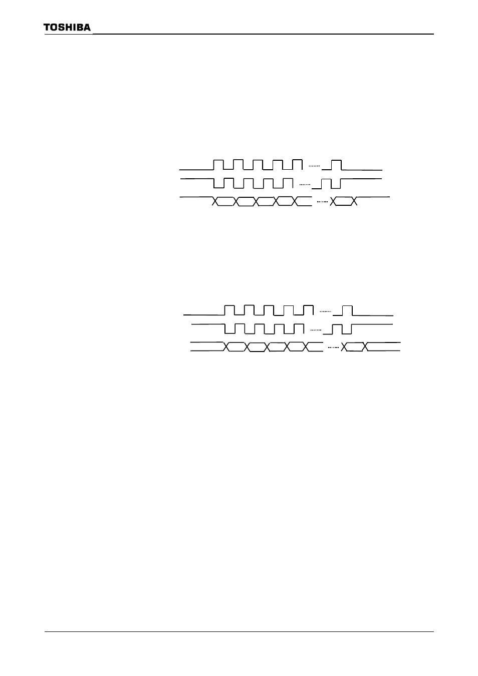
Select the edge of synchronous clock.
Please change the setting when
Figure 3.17.4
(e)
Select the edge of synchronous clock during receiving.
Please change the setting during SPIMD
Figure 3.17.5
(f)
Select logical invert/no invert when outputs transmitted data from SPDO pin.
Please don't change the setting of this register when transmitting/receiving is in
operation.
(g)
Select logical invert/no invert for received data from SPDI pin.
Please don't change the setting of this register when transmitting/receiving is in
operation.
SPDO pin
Bit0
Bit1
Bit2
Bit3
Bit4
Bit7
MSB
SPCLK pin (
= “1”)
LSB
SPCLK pin (
= “0”)
LSB
SPCLK pin (
SPDI pin
Bit0
Bit1
Bit2
Bit3
Bit4
MSB
SPCLK pin (