Toshiba H1 Series User Manual
Page 525
TMP92CZ26A
92CZ26A-522
LCDCTL0
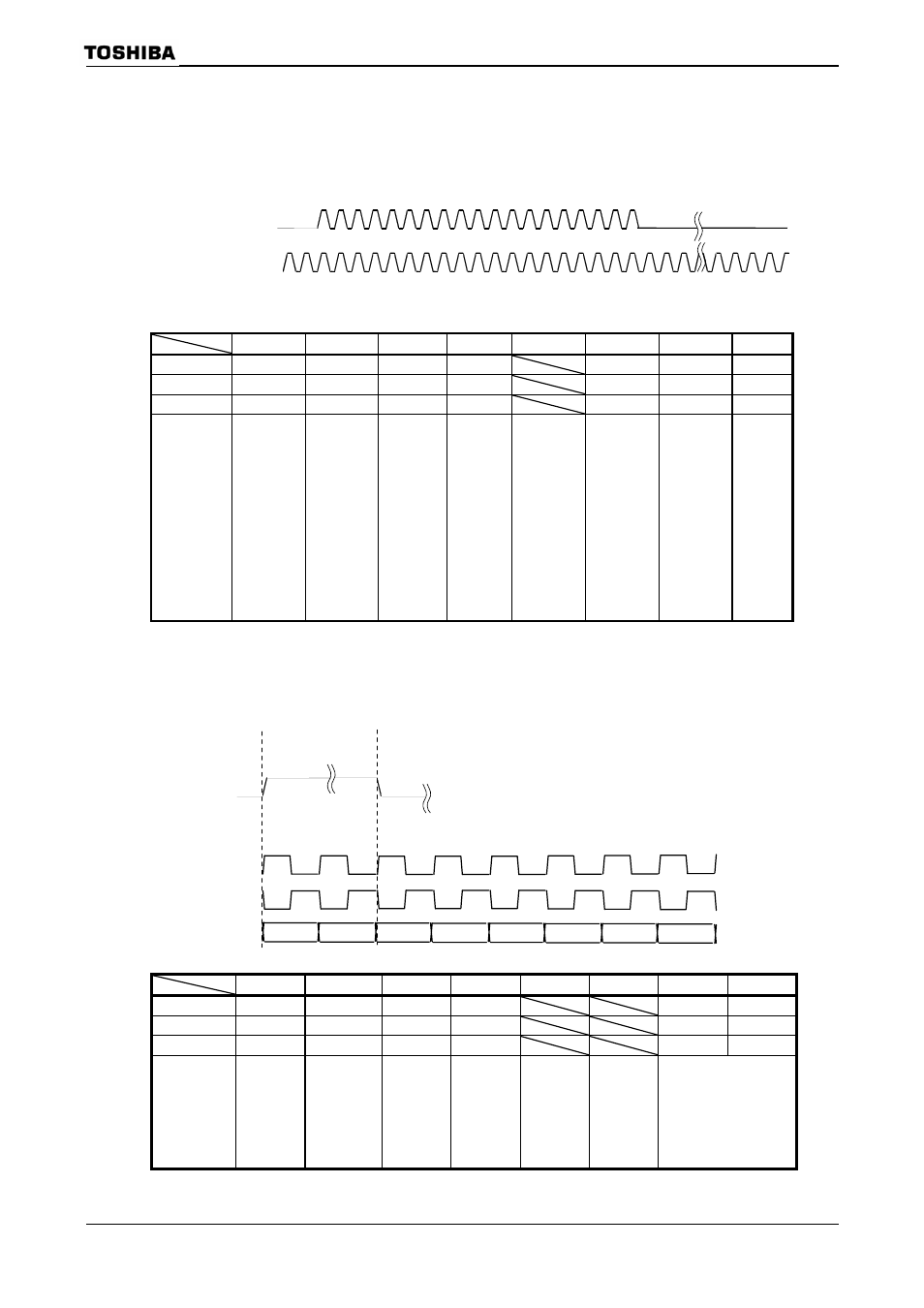
signal is output only when valid data is output.
LCD Control 0 Register
7 6 5
4 3 2 1
0
bit Symbol
PIPE
ALL0
FRMON
–
DLS
LCP0OC
START
Read/Write R/W
R/W
R/W R/W
R/W
R/W R/W
After reset
0
0
0
0
0
0
0
Function
PIP function
0: Disable
1: Enable
Segment
data
0: Normal
1: Always
output “0”
Frame divide
setting
0: Disable
1: Enable
Always
write “0”
FR
signal
LCP0/Line
selection
0: Line
1: LCP0
LCP0 (Note)
0: Always
output
1: At valid
data only
LLOAD
width
0: At setting
in register
1: At valid
data only
LCDC
operation
0: Stop
1: Start
Note: When select STN mode, LCP0 is output at valid data only regardless of the setting of
The phase of the LCP0 signal can be inverted by the setting of LCDCTL1
LCD Control 1 Register
7 6 5 4 3 2 1 0
bit Symbol
LCP0P
LHSP
LVSP
LLDP
LVSW1
LVSW0
Read/Write R/W
R/W
R/W R/W
R/W R/W
After reset
1
0
1
0
0
0
Function
LCP0
phase
0: Rising
1: Falling
LHSYNC
phase
0: Rising
1: Falling
LVSYNC
phase
0: Rising
1: Falling
LLOAD
phase
0: Rising
1: Falling
LVSYNC
enable time control
00 : 1 clock of LHSYNC
01 : 2 clocks of LHSYNC
10 : 3 clocks of LHSYNC
11 : Reserved
LCP0 signal LCP0OC=1
LCP0 signal LCP0OC=0
LCP0
LD23-LD0
LCP0
LCP0P=1
LCP0P=0
LVSYNC
LHSYNC
LLOAD
LGOEn
LFR
All signal changes
LCDCTL1
(0286H)
LCDCTL0
(0285H)