Figure 3.14.15.), Figure 3.14.16.) – Toshiba H1 Series User Manual
Page 337
TMP92CZ26A
92CZ26A-334
b. Receiving
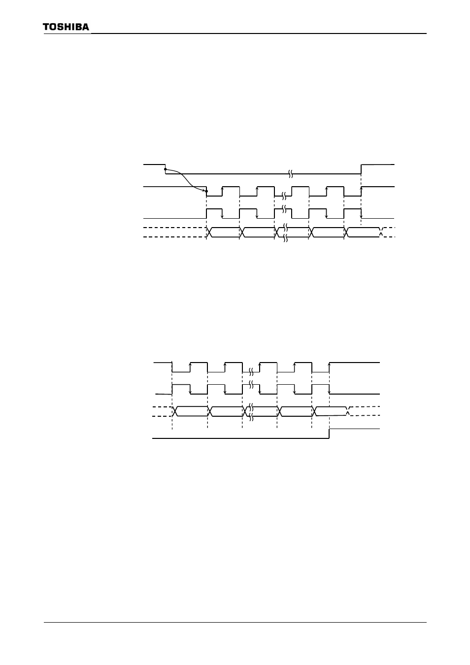
In SCLK Output Mode the synchronous clock is output on the SCLK0 pin and the
data is shifted to Receiving Buffer 1. This is initiated when the Receive Interrupt flag
INTES0
the data is transferred to Receiving Buffer 2 (SC0BUF) following the timing shown
below and INTES0
generated.
Setting SC0MOD0
Figure 3.14.15 Receiving operation in I/O Interface Mode (SCLK0 Output Mode)
In SCLK Input Mode the data is shifted to Receiving Buffer 1 when the SCLK input
goes active. The SCLK input goes active when the Receive Interrupt flag INTES0
is shifted to Receiving Buffer 2 (SC0BUF) following the timing shown below and
INTES0
Figure 3.14.16 Receiving Operation in I/O interface Mode (SCLK0 Input Mode)
Note: The system must be put in the Receive Enable state (SC0MOD0
SCLK0 output
(
rising edge mode)
IRX0C
(INTRX0 interrupt
request)
RXD0
Bit0
Bit1 Bit6
Bit7
SCLK0 output
(
falling edge mode)
SCLK0 input
(
= 0:
rising edge mode)
SCLK0 input
(
= 1:
falling edge mode)
IRX0C
(INTRX0 interrupt request)
RXD1
Bit1
Bit6
Bit7
Bit5
Bit