Serial bus interface control register 1, Figure 3.15.5 registers for the i, C bus mode table 3.15.1resolution of base clock – Toshiba H1 Series User Manual
Page 351: Clock gear base clock resolution
TMP92CZ26A
92CZ26A-348
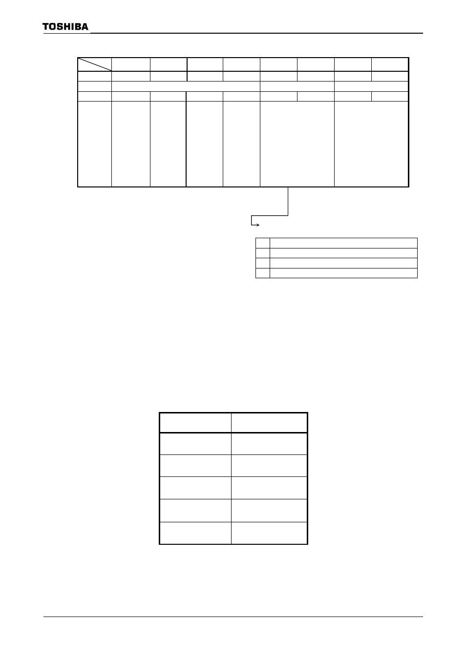
Serial Bus Interface Control Register 1
7 6 5 4 3 2 1 0
Bit symbol
MST
TRX
BB
PIN
SBIM1
SBIM0
SWRST1
SWRST0
SBICR2
(1243H)
Read/Write
W
W (Note 1)
W (Note 1)
After
reset
0 0 0 1 0 0 0 0
Prohibit
Read-
modify-
write
Function Master/Slave
selection
0:Slave
1:Master
Transmitter
/Receiver
selection
0:Receiver
1:Transmitter
Start/Stop
condition
Generation
0:Generate
stop
condition
1:Generate
start
condition
Cancel
INTSBI
interrupt
request
0:Don’t care
1:Cancel
interrupt
request
Serial bus interface
operating mode selection
(Note 2)
00: Port mode
01: (Reserved)
10: I
2
C Bus mode
11: (Reserved)
Software reset generate
write “10” and “01”, then
an internal reset signal is
generated.
Serial bus interface operating mode selection (Note2)
00
Port Mode (Serial Bus Interface output disabled)
01
Reserved
10
I
2
C Bus Mode
11
Reserved
Note 1: Reading this register functions as SBISR register.
Note 2: Switch a mode to port mode after confirming that the bus is free.
Switch a mode between I
2
C bus mode and port mode after confirming that input signals via port are
high-level.
Figure 3.15.5 Registers for the I
2
C bus mode
Table 3.15.1Resolution of base clock
@f
SYS
= 80MHz
Clock Gear
Base Clock
Resolution
000(fc)
f
SYS
/2
2
(50ns)
001(fc/2)
f
SYS
/2
3
(0.1us)
010(fc/4)
f
SYS
/2
4
(0.2us)
011(fc/8)
f
SYS
/2
5
(0.4us)
100(fc/16)
f
SYS
/2
6
(0.8us)