Toshiba H1 Series User Manual
Page 299
TMP92CZ26A
92CZ26A-296
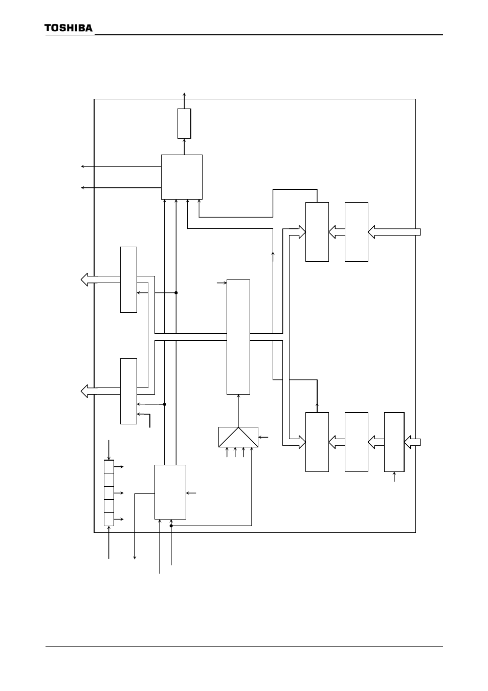
Figure 3.13.2 Block diagram of TMRB1
Internal data bus
Slelector
16-bit comparato
r
(CP12)
TB1MOD
φT1
φT4
φT16
Ti
mer
flip-
flop
control
TB1FF
0
TB1OUT0
Match
detection
16-bit timer regis
ter
TB1R
G0H/L
Register buffer
1
2
TA3O
UT
TB1MO
D
16-bit time register
TB1R
G1H/L
TB1MO
D
16-bit comparato
r
(CP13)
Capture,
external interrupt
input control
TB1RUN<
TB1R
UN>
Caputure registe
r
1
TB1CP1H/L
Capture register 0
TB1CP0H/L
Run/
clear
Internal data bus
Match detection
16-bit up counter
(UC12
)
Count
clock
(from TMRA01
)
Pr
escaler
clock
φT0
TMR
32
16
8
4
2
φT1
φT4
φT16
TB1RUN
Internal data bus
TB1MOD
Intenal data bus
Ti
me
r
flip-
flop
Ti
mer fl
ip
-fl
op
output
Interrup
t output
register 0
INTTB10
register 1
INTTB11
TB1RUN
External INT
in
put
INT7
TB1IN0