Toshiba H1 Series User Manual
Page 132
TMP92CZ26A
92CZ26A-129
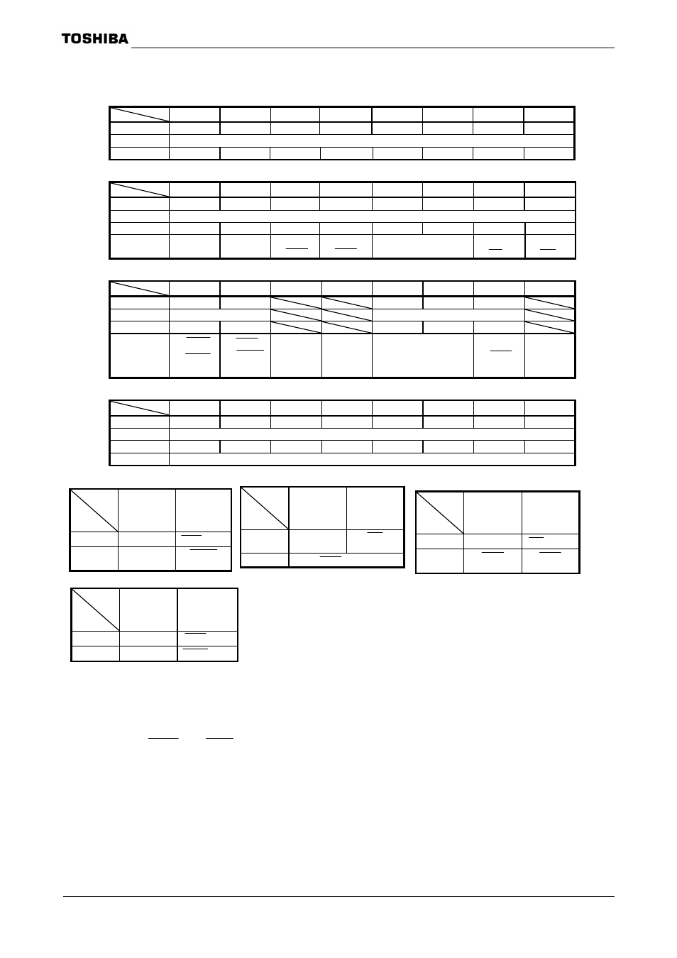
Port 8 register
7 6 5 4 3 2 1 0
bit Symbol
P87 P86 P85 P84 P83 P82 P81 P80
Read/Write R/W
After reset
1
1
1
1
1
0 (Note3)
1
1
Port 8 Function register
7 6 5 4 3 2 1 0
bit Symbol
P87F P86F P85F P84F P83F P82F P81F P80F
Read/Write W
After
reset 0 0 0 0 0 0 0 0
Function
0: Port
1:
0: Port
1:
0: Port
1:
CSZC
0: Port
1:
CSZB
Refer to following table
0: Port
1:
1
CS
0: Port
1:
0
CS
Port 8 Function registers 2
7 6 5 4 3 2 1 0
bit Symbol
P87F2 P86F2
P83F2 P82F2 P81F2
Read/Write W
W
After reset
0
0
0
0
0
Function
0:
CSXB
1:
CE
1
ND
0: CSZD
1:
CE
0
ND
Refer to following table
0:
1:
SDCS
Port 8 Drive register
7 6 5 4 3 2 1 0
bit Symbol
P87D P86D P85D P84D P83D P82D P81D P80D
Read/Write R/W
After
reset 1 1 1 1 1 1 1 1
Function
Input/Output buffer drive register for standby mode
Note1: Read-modify-write is prohibited for P8FC and P8FC2.
Note2: Don’t write “1” to P8
program memory by reset.
Note3: If it is started at boot mode (AM [1:0]
= “11”), output latch of P82 is set to “1”.
Note4: When
CE
0
ND
and
CE
1
ND
are used, set registers by following order.
Order Registser
bit2
bit1
------------------------------------------------------
(1) P8
1
1
(2) P8FC2
1
1
(3) P8FC
1
1
Figure 3.7.13 Register for Port 8
P8
(0020H)
P8FC
(0023H)
P8FC2
(0021H)
P8DR
(0088H)
0 1
0 Output
port
2
CS Output
1
CSZA
Output
SDCS
Output
P82 setting
0 1
0 Output
port
CSXB Output
1
Don’t setting
CE
1
ND
Output
P87 setting
0 1
0
Output port
CSZD
Output
1
Don’t setting
CE
0
ND
Output
P86 setting
0 1
0
Output
port
3
CS
Output
1
CSXA
Output
P83 setting