Serial bus interface control register 1, Figure 3.15.4 registers for the i, C bus mode – Toshiba H1 Series User Manual
Page 350
TMP92CZ26A
92CZ26A-347
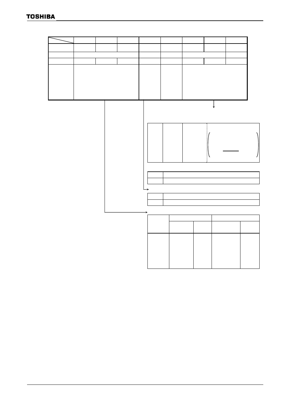
Serial Bus Interface Control Register 1
7 6 5 4 3 2 1 0
Bit symbol
BC2
BC1
BC0
ACK
−
SCK2 SCK1
SCK0/
SWRMON
Read/Write R/W R/W
R
R/W
R/W
After
Reset
0 0 0 0 1 0 0
0/1
(Note2)
Function
Number of transferred bits
(Note 1)
Acknowledge
mode
specification
0: Not
generate
1: Generate
Always
read as
“1”.
Internal serial clock selection and
software reset monitor
Internal serial clock selection
f
SYS
=80MHz (Output to SCL pin), Clock gear = fc/1
000
001
010
011
100
101
110
111
n
= 4
n
= 5
n
= 6
n
= 7
n
= 8
n
= 9
n
= 10
(Reserved)
−
−
−
−
68 kHz
36 kHz
18 kHz
(Reserved)
System Clock: f
SYS
(
=80MHz)
Clock Gear : fc/1
fscl
= [Hz]
Software reset state monitor
0
During software reset
1 (Initial
Data)
Acknowledge mode specification
0
Not generate clock pulse for acknowledge signal
1
Generate clock pulse for acknowledge signal
Number of bits transferred
= 0
= 1
Number of
clock pulses
Bits Number
of
clock pulses
Bits
000
001
010
011
100
101
110
111
8
1
2
3
4
5
6
7
8
1
2
3
4
5
6
7
9
2
3
4
5
6
7
8
8
1
2
3
4
5
6
7
Note1: For the frequency of the SCL line clock, see 3.15.5 (3) Serial clock.
Note2: The initial data of SCK0 is “0”, the initialdata of SWRMON is “1” if SBI operation is enable
(SBICR0
=“1”). If SBI operation is disable (SBICR0
Note3: This I
2
C bus circuit does not support Fast-mode, it supports the Standard mode only. Although the I
2
C bus
circuit itself allows the setting of a baud rate over 100kbps, the compliance with the I
2
C specification is not
guaranteed in that case.
Figure 3.15.4 Registers for the I
2
C bus mode
SBICR1
(1240H)
Prohibit
Read-
modify-
write
f
SYS
/4
2
n
+ 35