Figure3.10.4 single write cycle timing, Figure3.10.5 burst write cycle timing – Toshiba H1 Series User Manual
Page 229
TMP92CZ26A
92CZ26A-226
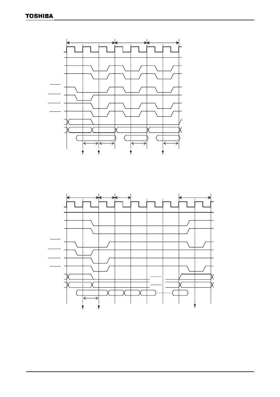
Figure3.10.4 Single Write Cycle Timing
Figure3.10.5 Burst Write Cycle Timing
SDCLK
SDCKE
SDLUDQM
SDLLDQM
A10
A15-A0
D15-D0
RA
Bank
Active
RA
CA (n)
CA (n+2)
D (n+2)
Write
tRCD=
1CLK
3CLK
2CLK
tWR=
1CLK
D (n)
tWR=
1CLK
D (n+4)
tWR=
1CLK
CA (n+4)
2CLK
Write
Write
SDCS
SDRAS
SDCAS
SDWE
SDCLK
SDCKE
SDLUDQM
SDLLDQM
A10
A15-A0
D15-D0
RA
Bank
Active
RA
CA(n)
D(n+2)
Write
tRCD=
1CLK
2CLK
1CLK
D(n)
D(n+4)
1CLK
Burst
Stop
A10
A15-0
Burst Stop Cycle 2CLK
D(n+6)
D(end)
CA(n)
SDCS
SDRAS
SDCAS
SDWE
This manual is related to the following products: