Figure 3.23.3 ad converter related register – Toshiba H1 Series User Manual
Page 600
TMP92CZ26A
92CZ26A-597
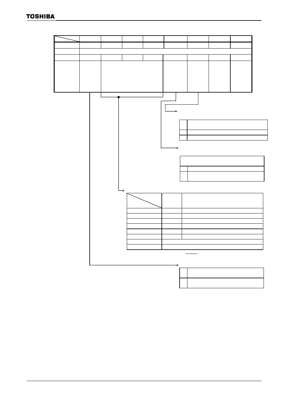
AD Mode Control Register 1 (Normal conversion control)
7 6 5 4 3 2 1 0
bit Symbol
DACON
ADCH2
ADCH1
ADCH0
LAT
ITM
REPEAT
SCAN
Read/Write R/W
After
reset
0 0 0 0 0 0 0 0
Function
DAC and
VREF
application
control
Analog input channel select
Latency
0: No Wait
1:Start after
reading
conversion
result store
Register of
last channel
Interrupt
specification
when
conversion
channel fixed
repeat mode
Repeat mode
specification
0: Single
conversion
1: Repeat
conversion
Scan mode
specification
0: Channel
fixed mode
1: Channel
scan mode
Figure 3.23.3 AD Converter Related Register
ADMOD1
(12B9H)
Next SCAN start timing control for the channel
scan repeat mode
Channel Scan Repeat mode
(
= 1,
0
No Wait
1
Start after read last of conversion result
store Register
Specify AD conversion interrupt for Channel Fixed
Repeat Conversion mode
Channel Fixed Repeat Conversion Mode
= “0”,
0
Generates interrupt every conversion
1
Generated interrupt every fourth conversion
DAC & VREF application control
0
DAC & VREF off
(Set before into STOP mode)
1
DAC & VREF on
(Set to “1” before starting conversion)
Analog input channel select
0:
Channel
fixed
1:
Channel scanned
000 AN0
AN0
001 AN1
AN0
→AN1
010 AN2
AN0
→AN1→AN2
011 AN3(note)
AN0
→AN1→AN2→AN3 (note)
100 AN4
AN0
→AN1→AN2→AN3→AN4 (note)
101 AN5
AN0
→AN1→AN2→AN3→AN4→AN5 (note)
110 Reserved
111 Reserved
Note: When using PG3 pin as
ADTRG
, it cannot be set.