1 block diagram – Toshiba H1 Series User Manual
Page 500
TMP92CZ26A
92CZ26A-497
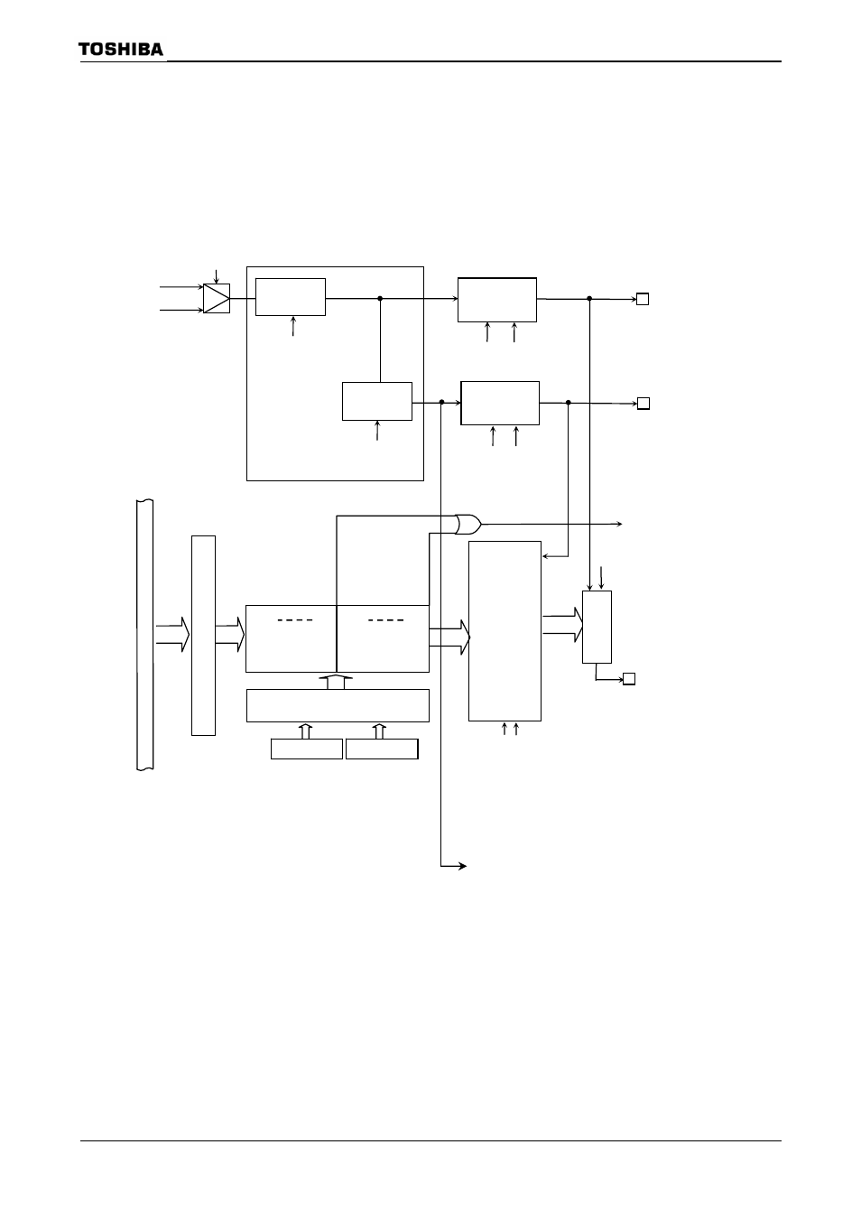
3.18.1 Block
Diagram
The I
2
S unit contains two channels: channel 0 and channel 1. Each channel can be controlled
and made to output independently.
Figure 3.18.1 shows a block diagram for I
2
S channel 0.
Figure 3.18.1 I
2
S Block Diagram
f
SYS
I2SCKO
Control
I2S0CTL
I2S0CKO
I2SWS
Control
I2S0CTL
WLVL0> I2S0WS 64-byte FIFO0 32) 0 1 31 Data Selector Interrupt Control I2S0DO Read Pointer FIFO Control I2SBUF0 INTI2S0 32bit I2S0CTL I2S0CTL Shifter Internal Data Bu s Write Pointer 8-bit Counter I2S0C I2S0C 6-bit Counter Clock Generator 64-byte FIFO1 32) 0 1 31 f I2S Request Signal Output to ADC (Supported in channel 0 only) I2S0CTL
(2 bytes
(2 bytes
This manual is related to the following products: