2 sfr, Figure 3.3.3 sfr for system clock – Toshiba H1 Series User Manual
Page 27
TMP92CZ26A
92CZ26A-24
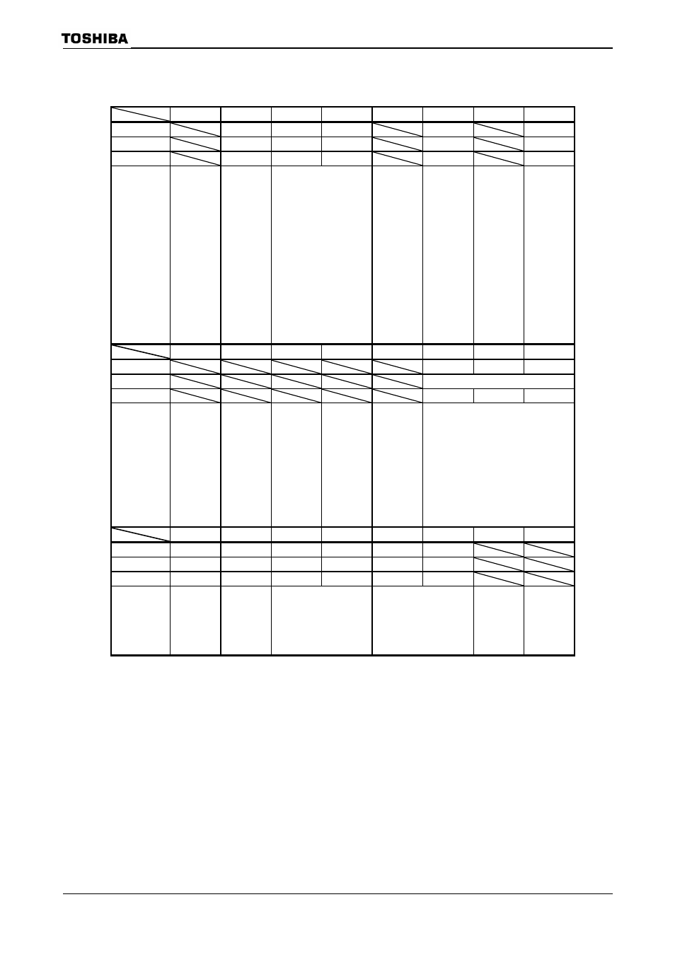
3.3.2 SFR
7 6 5 4 3 2 1 0
bit Symbol
XTEN
USBCLK1
USBCLK0
WUEF PRCK
Read/write
R/W
R/W
R/W R/W R/W
After Reset
1
0
0
0
0
Function
Low
-frequency
oscillator
circuit (fs)
0: Stop
1: Oscillation
Select the clock of
USB(f
USB
)
00:Disable
01: Reserved
10:X1USB
11:f
PLLUSB
Warm-up
Timer
0: Write
Don’t care
Note3
1: Write
start timer
0: Read
end
warm-up
1: Read
do not end
warm-up
Select
Prescaler
clock
0: f
SYS
/2
1: f
SYS
/8
7 6 5 4 3 2 1 0
bit
Symbol
GEAR2
GEAR1
GEAR0
Read/write
R/W
After
Reset
1
0
0
Function
Select gear value of high frequency (fc)
000: fc
001: fc/2
010: fc/4
011: fc/8
100: fc/16
101: Reserved
110: Reserved
111: Reserved
7 6 5 4 3 2 1 0
bit Symbol
–
CKOSEL WUPTM1
WUPTM0
HALTM1
HALTM0
Read/write
R/W R/W R/W R/W R/W R/W
After
Reset
0 0 1 0 1 1
Function
Always
write “0”
Select
CLKOUT
0: f
SYS
1: f
S
Warm-Up Timer
00: reserved
01: 2
8
/inputted frequency
10:2
14
/inputted frequency
11:2
16
/inputted frequency
HALT mode
00: Reserved
01: STOP mode
10: IDLE1 mode
11: IDLE2 mode
Note1: SYSCR0
Note2: By reset, low frequency oscillator circuit is enabled.
Note3: Don’t write SYSCR0 resiter during warming up. Because the warm-up end flag doesn’t become enable if
write ”0” to SYSCR0
( Read-modify-write is prohibited for SYSCR0 register during warming up.)
Figure 3.3.3 SFR for system clock
SYSCR0
(10E0H)
SYSCR1
(10E1H)
SYSCR2
(10E2H)