Maps and registers, 1 fpga registers, Table 5-1 – Artesyn ATCA-7480 Installation and Use (February 2015) User Manual
Page 99: Register default, Table 5-2, Register access type, Chapter 5
Chapter 5
ATCA-7480 Installation and Use (6806800T17A)
99
Maps and Registers
5.1
FPGA Registers
For register description, the convention shown in
are used.
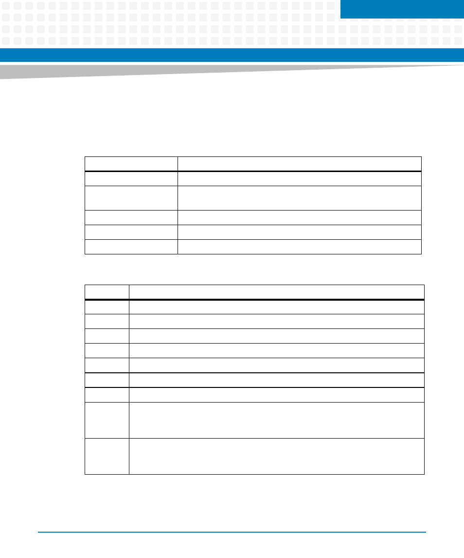
Table 5-1 Register Default
Default
Description
-
Not applicable or undefined
0 or 1
Default value after PWR_GOOD is valid or after PCH_PLTRST_
deassertion.
Undef.
Undefined value
Default value after deassertion of the reset signal
Ext.
External Reset Source. Default depends on external logic level.
Table 5-2 Register Access Type
Access
Description
r
Read only
w
Write only
r/w
Read and write
w1c
Write-1-to-clear, ignore bit while reading
r/w1c
Read and write-1-to-clear, write 0 has no effect
r/w1s
Read and write-1-to-set, write 0 has no effect
r/w1t
Read and write-1-to-toggle, write 0 has no effect
LPC:
The prefix “LPC:” signals that the access is restricted to the LPC interface.
For example, LPC: r/w means that the register bit is readable/writable from the LPC
interface
IPMC:
The prefix “IPMC:” signals that the access is restricted to the IPMC I2C interface.
For example, IPMC: r/w means that the register bit is readable/writable from IPMC I2C
interface