4 uart1 and uart2 register map, 1 uart register overview, Table 5-20 – Artesyn ATCA-7480 Installation and Use (February 2015) User Manual
Page 109: Logical device 0x74 reserved register, Table 5-21, Logical device 0x75 reserved register, Table 5-22, Logical device 0xf0 reserved register, Maps and registers
Maps and Registers
ATCA-7480 Installation and Use (6806800T17A)
109
5.1.4
UART1 and UART2 Register Map
The LPC IO Base addresses BASE1 for UART1 and BASE2 for UART2 are set up during Super IO
configuration. See
Super IO Configuration Register
5.1.4.1
UART Register Overview
shows the registers and their addresses as offsets of a base address for one of the
two UARTs.
The state of the Divisor Latch Bit (DLAB), which is the MOST significant bit of the Serial Line
Control Register (SCR), affects the selection of certain of the UART registers. The DLAB bit must
be set high by the system software to access the Baud Rate Generator Divisor Latches (DLL and
DLM).
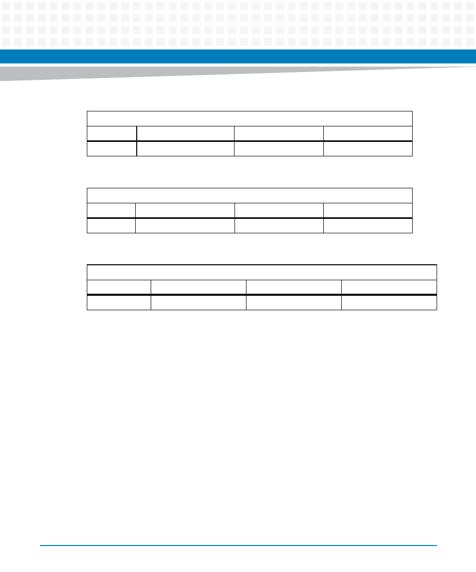
Table 5-20 Logical Device 0x74 Reserved Register
Index Address: 0x74
Bit
Description
Default
Access
7:0
Reserved
0x04
LPC: r
Table 5-21 Logical Device 0x75 Reserved Register
Index Address: 0x75
Bit
Description
Default
Access
7:0
Reserved
0x04
LPC: r
Table 5-22 Logical Device 0xF0 Reserved Register
Index Address: 0xF0
Bit
Description
Default
Access
7:0
Reserved
0
LPC: r