Transmit clock counter (escc only), Clock selection – Zilog Z80230 User Manual
Page 90
SCC/ESCC
User Manual
UM010903-0515
SCC/ESCC Ancillary Support Circuitry
83
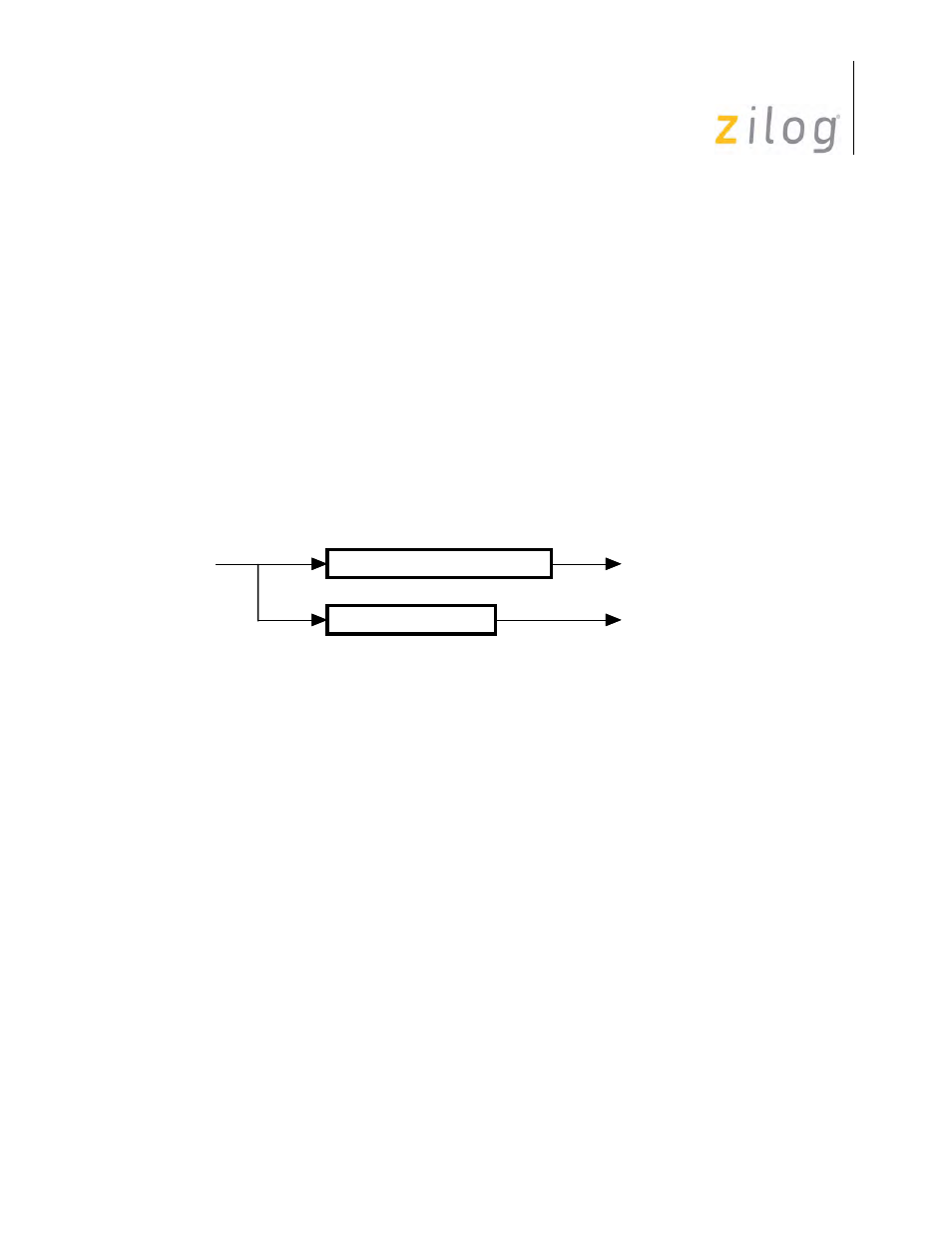
Transmit Clock Counter (ESCC only)
The ESCC includes a Transmit Clock Counter which parallels the DPLL. This counter provides a
jitter-free clock source to the transmitter by dividing the DPLL clock source by the appropriate
value for the programmed data encoding format as displayed in
. Therefore, in FM mode
(FM0 or FM1), the counter output is the input frequency divided by 16. In NRZI mode, the coun-
ter frequency is the input divided by 32. The counter output replaces the DPLL transmit clock out-
put, available as the transmit clock source. This has no effect on the use of the DPLL as the receive
clock source.
The output of the transmit clock derived from this counter is available to the /TRxC pin when the
DPLL output is selected as the transmit clock source. Care must be taken using ESCC in SDLC
Loop mode with the DPLL. The SDLC Loop mode requires synchronized Tx and Rx clocks, but
the ESCC’s DPLL might be off-sync because of this Transmit Clock Counter. In SDLC Loop, one
should instead echo the signal of the RxDPLL out to clock the receiver and transmitter to achieve
synchronization. This can be programmed via bits D1-D0 in WR11.
DPLL Transmit Clock Counter Output (ESCC only)
Clock Selection
The SCC can select several clock sources for internal and external use. Write Register 11 is the
Clock Mode Control register for both the receive and transmit clocks. It determines the type of
signal on the /SYNC and /RTxC pins and the direction of the /TRxC pin.
The SCC is programmed to select one of several sources to provide the transmit and receive
clocks.
The source of the receive clock is controlled by bits D6 and D5 of WR11. The receive clock may
be programmed to come from the /RTxC pin, the /TRxC pin, the output of the baud rate generator,
or the receive output of the DPLL.
The source of the transmit clock is controlled by bits D4 and D3 of WR11. The transmit clock may
be programmed to come from the /RTxC pin, the /TRxC pin, the output of the baud rate generator,
or the transmit output of the DPLL.
DPLL
DPLL Counter
Input Divided by 16 (FM0 or FM1)
Input Divided by 32 for NRZI
DPLL Output to Receiver
DPLL Output to Transmitter
DPLL CLK
Input