Write register 11 (clock mode control) – Zilog Z80230 User Manual
Page 172
SCC/ESCC
User Manual
UM010903-0515
Register Descriptions
165
mode operation in other registers are set before this mode is selected. The transmitter and receiver
are not enabled until after this mode has been selected. As soon as the Go-Active-On-Poll bit is set
and an EOP is received, the SCC goes on-loop. If this bit is reset after the SCC goes on-loop, the
SCC waits for the next EOP to go off-loop.
In synchronous modes, the SCC uses this bit, along with the Go-Active-On-Poll bit, to synchro-
nize the transmitter to the receiver. The receiver should not be enabled until after this mode is
selected. The TxD pin is held marking when this mode is selected unless a break condition is pro-
grammed. The receiver waits for a sync character to be received and then enables the transmitter
on a character boundary. The break condition, if programmed, is removed. This mode works prop-
erly with sync characters of 6, 8, or 16 bits. This bit is ignored in Asynchronous mode and is reset
by a channel or hardware reset.
Bit 0: 6-Bit/8-Bit SYNC select bit
This bit is used to select a special case of synchronous modes. If this bit is set to 1 in Monosync
mode, the receiver and transmitter sync characters are six bits long instead of the usual eight. If
this bit is set to 1 in Bisync mode, the received sync is 12 bits and the transmitter sync character
remains 16 bits long. This bit is ignored in SDLC and Asynchronous modes, but still has effect in
the special external sync modes. This bit is reset by a channel or hardware reset.
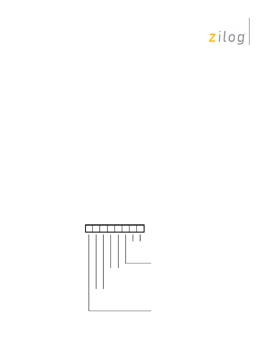
Write Register 11 (Clock Mode Control)
WR11 is the Clock Mode Control register. The bits in this register control the sources of both the
receive and transmit clocks, the type of signal on the /SYNC and /RTxC pins, and the direction of
the /TRxC pin. Bit positions for WR11 are displayed in
; also, see
D7 D6 D5 D4 D3 D2 D1 D0
Write Register 11
0 0 /TRxC Out = Xtal Output
0 1 /TRxC Out = Transmit Clock
1 0 /TRxC Out = BR Generator Output
1 1 /TRxC Out = DPLL Output
/TRxC O/I
0 0 Transmit Clock = /RTxC Pin
0 1 Transmit Clock = /TRxC Pin
1 0 Transmit Clock = BR Generator Output
1 1 Transmit Clock = DPLL Output
0 0 Receive Clock = /RTxC Pin
0 1 Receive Clock = /TRxC Pin
1 0 Receive Clock = BR Generator Output
1 1 Receive Clock = DPLL Output
/RTxC Xtal//No Xtal