Sram write cycle – Zilog Z80230 User Manual
Page 223
SCC/ESCC
User Manual
UM010903-0515
Application Notes
216
No wait states are necessary if there is a 85 ns, or faster, access time by using SRAMs. Since the
Z180 has on-chip MMU with 85 ns or faster SRAM just copy the contents of EPROM (application
program starts at logical address
0000h
) into SRAM after power on. Set up the MMU to SRAM
area to override the EPROM area and stop inserting wait states. With this scheme, you can get the
highest performance with moderate cost.
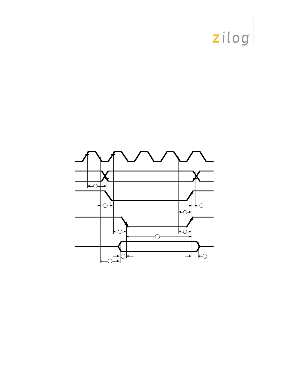
SRAM Write Cycle
During a Z180 memory write cycle, the Z180 write data is stable before the falling edge of /WR
(Z180 parameter #24; 15 ns min at 10 MHz). It is stable throughout the write cycle (Z180 parame-
ter #27; 10 ns min at 10 MHz). Further, the address is fixed before the falling edge of /WR. The /
WR pulse width meets the SRAM’s spec (see Table on page 214).
Z180 Memory Write Cycle Timing (One Wait State)
Memory Interface Logic
The memory devices (EPROM and SRAM) for this design are 256 kb (32 KB). There are two pos-
sible memory interface designs:
Connect Address Decode output to /E input. Put the signal generated by /RD and /MREQ ANDed
together to /OE of EPROM and SRAM. Put the signal generated by /WR and /MREQ ANDed
together to the /WE pin of SRAM (Figure on page 217).
6
22
12
11
26
25
27
Ø
Address
/MREQ
/WR
Data
T1
T2
Tw
T3
T1
8
24
23