Zilog Z80230 User Manual
Page 167

SCC/ESCC
User Manual
UM010903-0515
Register Descriptions
160
at the same time as the Reset command, because these bits are only reset by a hardware reset. Bit
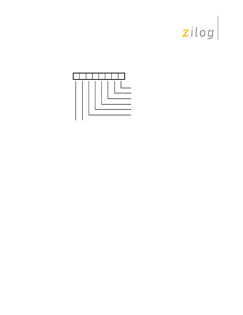
positions for WR9 are displayed in
.
Write Register 9
Bit 7 and 6: Reset Command Bits
Together, these bits select one of the reset commands for the SCC. Setting either of these bits to 1
disables both the receiver and the transmitter in the corresponding channel; forces TxD for that
channel marking, forces the modem control signals High in that channel, resets all IPs and IUSs
and disables all interrupts in that channel. Four extra PCLK cycles must be allowed beyond the
usual cycle time after any of the reset commands is issued before any additional commands or
controls are written to the channel affected.
Null Command (00).
This command has no effect. It is used when a write to WR9 is necessary for
some reason other than an SCC Reset command.
Channel Reset B Command (01).
Issuing this command causes a channel reset to be performed
on Channel B.
Channel Reset A Command (10).
Issuing this command causes a channel reset to be performed
on Channel A.
Force Hardware Reset Command (11).
The effects of this command are identical to those of a
hardware reset, except that the Shift Right/Shift Left bit is not changed and the MIE, Status High/
Status Low and DLC bits take the programmed values that accompany this command.
Bit 5: Software Interrupt Acknowledge control bit
If bit D5 is set, reading Read Register 2 (RR2) results in an interrupt acknowledge cycle to be exe-
cuted internally. Like a hardware INTACK cycle, a software acknowledge causes the INT pin to
return High, the IEO pin to go Low, and sets the IUS latch for the highest priority interrupt pend-
ing.
D7 D6 D5 D4 D3 D2 D1 D0
Write Register 9
VIS
0 0 No Reset
0 1 Channel Reset B
1 0 Channel Reset A
1 1 Force Hardware Reset
NV
DLC
MIE
Status High//Status Low
Software INTACK Enable
(Reserved on NMOS)
