Scc/escc user manual – Zilog Z80230 User Manual
Page 229
SCC/ESCC
User Manual
UM010903-0515
Application Notes
222
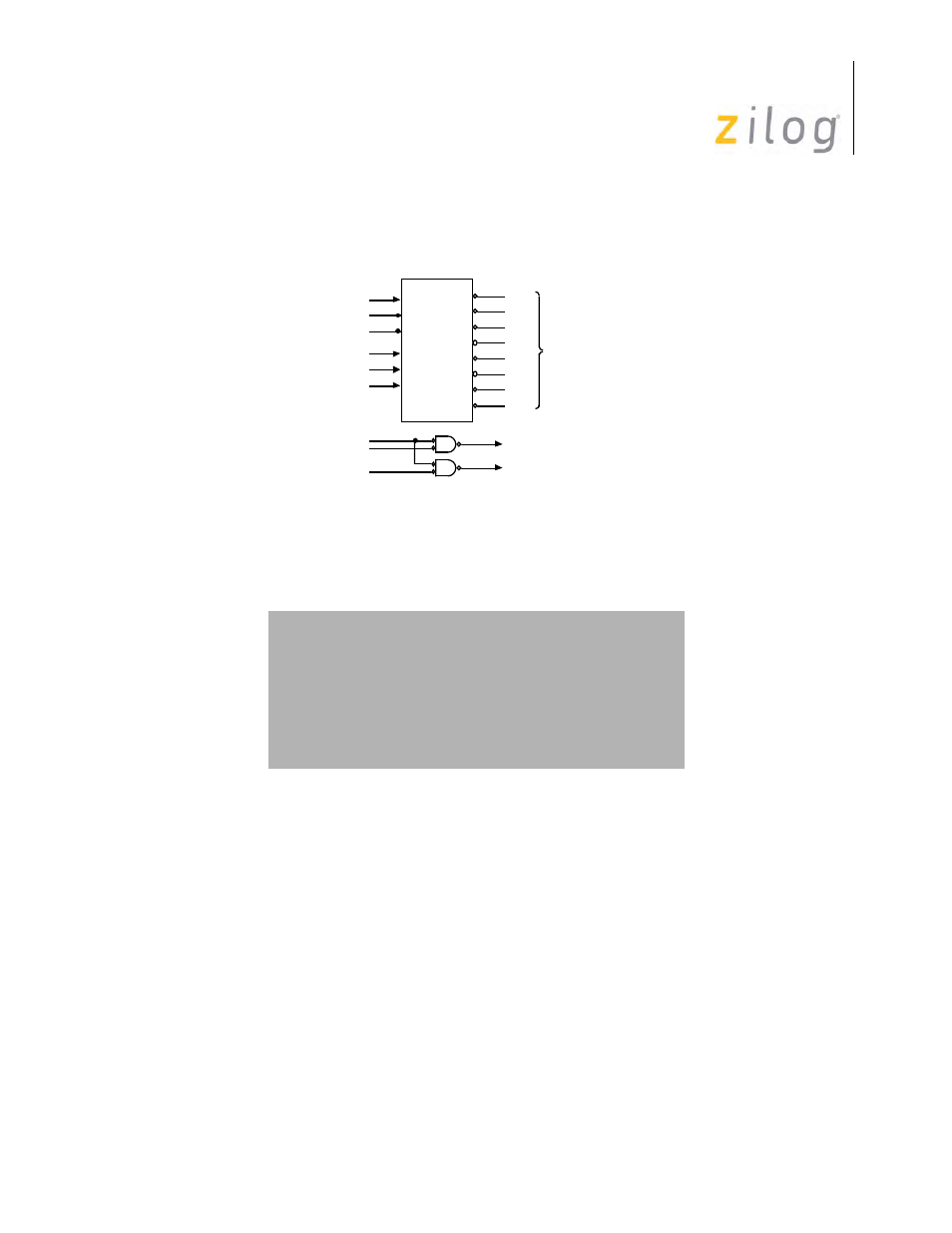
Figure displays a simple address decoder (the required interface signals, other than address decode out-
puts, are discussed in the following sections).
I/O Interface Logic (Example)
I/O Address Decoder for this Board
When expanding this board to enable other peripherals, the decoded address A6/A7 is NANDed
with USRIO to produce the Chip Enable (CSSCC) output signal (HC10). The SCC registers are
assigned from address
xxC0h
to
xxC3h
; with image, they occupy
xxC0h
to
xxFFh
. To add wait
states during I/O transactions, use the Z180 on-chip wait state generator instead of external hard-
ware logic.
If there is a Z80
®
PIO on board in a Z-mode of operation (that is, clear /M1E in OMCR register to
zero) and after enabling a Z80 PIO interrupt, zero is written to M1TE in the OMCR register. With-
out a zero, there is no interrupt from the Z80 PIO. The Z80 PIO requires /M1 to activate an inter-
rupt circuit after enabling interrupt by software.
/G2A
/G2B
C
B
A
A17
A2
A5
A4
A3
/Y9
/Y6
/Y5
/Y4
/Y3
/Y2
/Y1
/Y0
50 ~
58 ~
54 ~
50 ~
40 ~
48 ~
44 ~
40 ~
HCT138
/IORQ
/RD
/WR
/IORD To Each
Peripherals' /RD
/IOWR To Each
Peripherals' /WR
A6
G1
Chip Select Signals
for Peripherals