Ttl output & trigger input configuration, Expanded memory configuration, Caution – Measurement Computing TempScan/1100 User Manual
Page 28
1-14 System Overview
899493
TempScan / MultiScan User's Manual
DB50 Digital I/O Pin Descriptions
Line
Pin
Line
Pin
Line
Pin
Line
Pin
Line
Pin
Output 1
1
Output 11
37
Output 21
24
Output 31
11
Ground
12
Output 2
34
Output 12
21
Output 22
8
Output 32
44
Ground
13
Output 3
18
Output 13
5
Output 23
41
Input 1
15
Ground
14
Output 4
2
Output 14
38
Output 24
25
Input 2
48
Ground
28
Output 5
35
Output 15
22
Output 25
9
Input 3
32
Ground
29
Output 6
19
Output 16
6
Output 26
42
Input 4
16
Ground
30
Output 7
3
Output 17
39
Output 27
26
Input 5
49
Ground
31
Output 8
36
Output 18
23
Output 28
10
Input 6
33
Ground
45
Output 9
20
Output 19
7
Output 29
43
Input 7
17
Ground
46
Output 10
4
Output 20
40
Output 30
27
Input 8
50
Ground
47
Each digital output line will drive five (5) standard TTL (transistor-transistor logic) loads. All digital input
lines are one-eighth (0.125) TTL loads. All inputs are protected against damage from high static voltage.
Normal precautions should be taken to limit the input voltages to the range of 0.0 to 5.3 volts. All digital
I/O lines are referenced to digital ground.
CAUTION
Do not exceed the levels described. Otherwise, the TempScan/1100 or
MultiScan/1200 unit may be damaged in a way that is not covered by the
warranty.
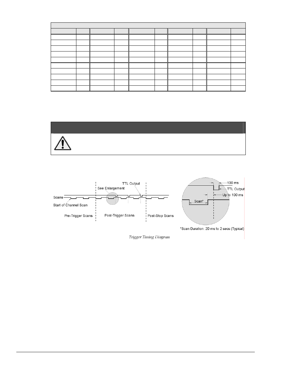
TTL Output & Trigger Input Configuration
The rear panel of the TempScan/1100 or MultiScan/1200 unit also provides two external BNC connectors:
The TTL output and the trigger input. The BNC TTL scan output is used for synchronizing equipment
with TempScan/1100 or MultiScan/1200 acquisition, while the BNC trigger input is used for starting
and/or stopping acquisition of the TTL output. This trigger input can be programmed to activate on a
rising (positive-going) or falling (negative-going) TTL level edge. Any TTL level signal
(> 2.2V = Hi, < 0.8V = Lo) may be used as a trigger pulse. A trigger pulse may also be used to generate a
Service Request. Note that the TTL Out is a LS-TTL compatible output, 0.4 mA sourcing, 8 mA sinking.
When a scan is logged into the acquisition buffer (after the actual scan), the TTL output signal is pulsed for
100 ms. Refer to the timing diagram.