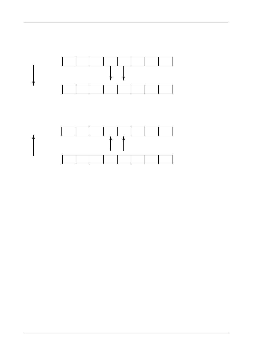
Figure49 hi flag operation, 6 hsr reserved—bits 5 and 6, 7 hsr dma status (dma)—bit 7 – Motorola DSP56012 User Manual
Page 98: 3 hi receive data register (horx), Hsr reserved—bits 5 and 6 -18, Hsr dma status (dma)—bit 7 -18, Hi receive data register (horx) -18, Figure 4-9, Hi flag operation -18, For additional information. an

4-18
DSP56012 User’s Manual
MOTOROLA
Parallel Host Interface
Host Interface (HI)
4.4.4.2.6
HSR Reserved—Bits 5 and 6
These status bits are reserved for future revisions and read as 0s during DSP read
operations.
4.4.4.2.7
HSR DMA Status (DMA)—Bit 7
The DMA bit indicates that the host processor has enabled the DMA mode of the HI
by setting HM1 or HM0 to 1. When the DMA bit is 0, it indicates that the DMA mode
is disabled by the HM0 and HM1 bits (in the ICR) and that no DMA operations are
pending. When the DMA bit is set, the DMA mode has been enabled if one or more
of the host mode bits have been set. The channel not in use can be used for polling or
interrupt operation by the DSP.
Note:
Hardware reset, software reset, individual reset, and Stop clear the DMA bit.
4.4.4.3
HI Receive Data Register (HORX)
The HI Receive data register (HORX) is used for host-to-DSP data transfers. The
HORX register is viewed as a 24-bit read-only register by the DSP CPU. The HORX
register is loaded with 24-bit data from the Transmit data registers (TXH:TXM:TXL)
on the host processor side when both the host-side Transmit Data register Empty
Figure 4-9 HI Flag Operation
Host to DSP56012 Status Flags
$0
Host
Interrupt Control Register
(ICR)
(Read/write)
Host Status Register
(HSR)
(Read Only)
DSP56012
INIT
HF1
HF0
0
TREQ
RREQ
7
0
HM0
HM1
X:$FFE9
DMA
HF1
HF0
HCP
HTDE
HRDF
7
0
0
0
DSP56012 to Host Status Flags
$2
Host
Interrupt Status Register
(ISR)
(Read Only)
Host Control Register
(HCR)
(Read/write)
DSP56012
HOREQ
HF3
HF2
TRDY
TXDE
RXDF
7
0
0
DMA
X:$FFE8
0
HF3
HF2
HCIE
HTIE
HRIE
7
0
0
0
AA0316
