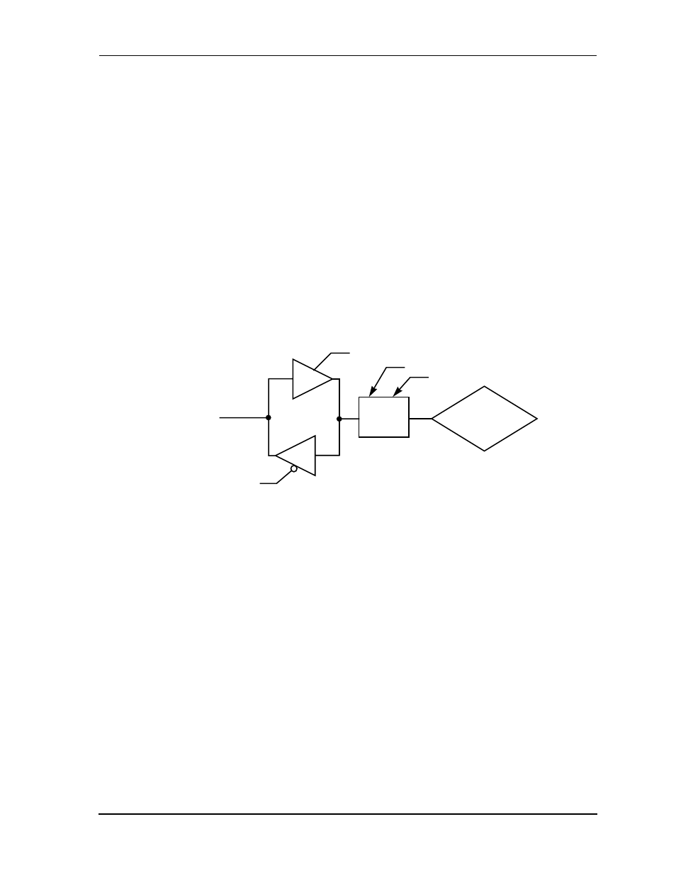
Figure72 gpio circuit diagram, Figure 7-2, Gpio circuit diagram -5 – Motorola DSP56012 User Manual
Page 209

GPIO
GPIO Register (GPIOR)
MOTOROLA
DSP56012 User’s Manual
7-5
• When the GCx bit is cleared and the GDDx bit is cleared (the pin is defined as
an input), the corresponding GPIOx pin input buffer is disconnected from the
pin and does not require an external pull-up (see
• When the GCx bit is set and the GDDx bit is cleared (the pin is defined as
input), the corresponding GPIOx pin input buffer is connected to the pin (see
and
• When the GCx bit is cleared and the GDDx bit is set (the pin is defined as
output), the corresponding GPIOx pin output buffer is defined as a standard
active high/active low type (see
• When the GCx bit is set and the GDDx bit is set (the pin is defined as output),
the corresponding GPIOx pin output buffer is defined as an open-drain type
(see
The GC[7:0] bits are cleared during hardware reset and software reset.
Figure 7-2 GPIO Circuit Diagram
GD0–GD7
PIN
GDD
GDD
GC
*
See
Table 7-1 GPIO Pin Configuration
Buffer
Control*
GDD
AA0442k
