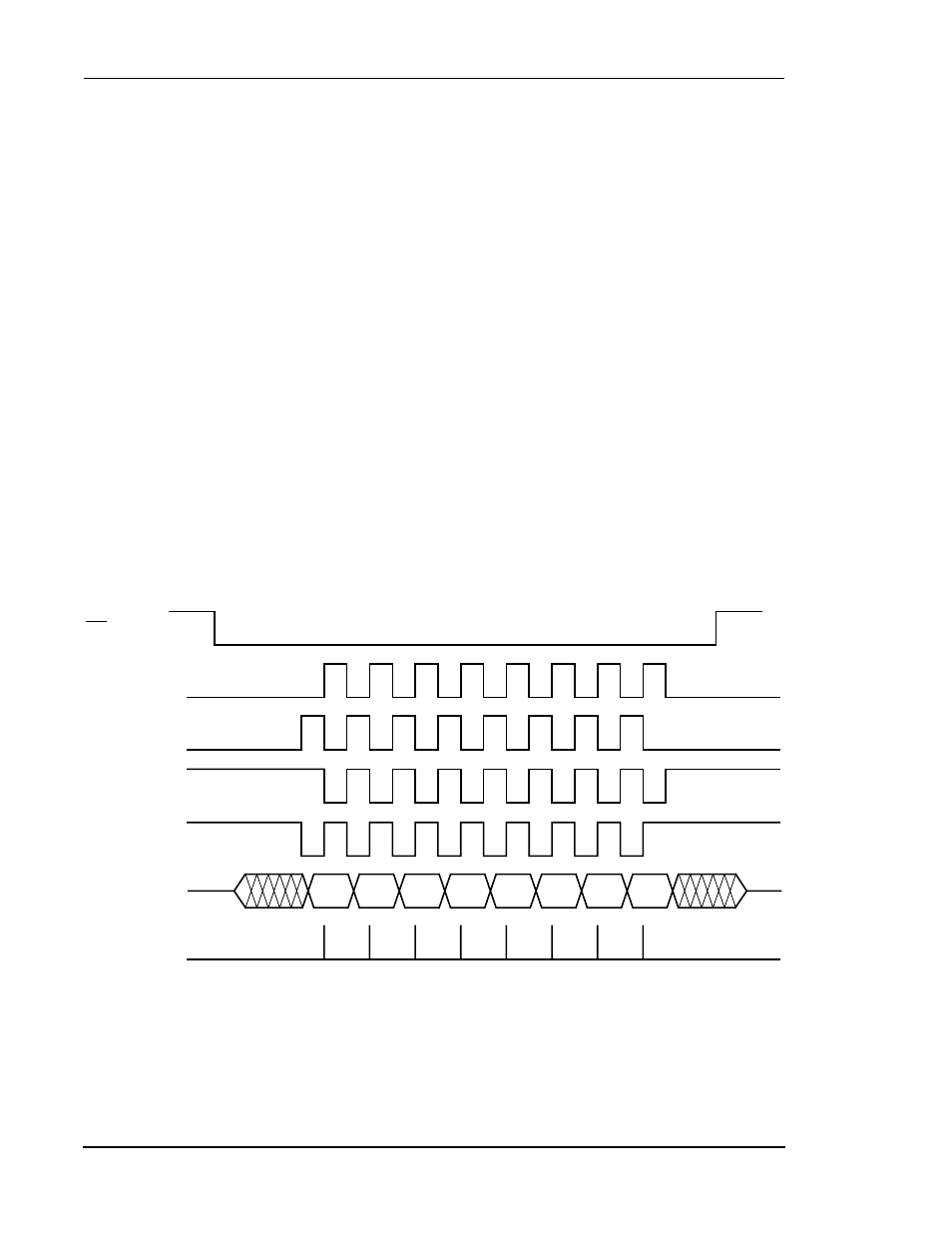
Figure56 spi data-to-clock timing diagram, Figure 5-6, Spi data-to-clock timing diagram -10 – Motorola DSP56012 User Manual
Page 158

5-10
DSP56012 User’s Manual
MOTOROLA
Serial Host Interface
Serial Host Interface Programming Model
Note:
The maximum-allowed internally generated bit clock frequency is
fosc
/
4
for
the SPI mode and
fosc
/
6
for the I
2
C mode (the maximum-allowed externally
generated bit clock frequency is
fosc
/
3
for the SPI mode and
fosc
/
5
for the I
2
C
mode). The programmer should not use the combination HRS = 1 and
HDM[5:0] = 000000, since it may cause synchronization problems and
improper operation (it is therefore considered an illegal combination).
Note:
The HCKR bits are cleared during hardware reset or software reset, except for
CPHA, which is set. The HCKR is not affected by the Stop state.
The HCKR bits are described in the following paragraphs.
5.4.5.1
Clock Phase and Polarity (CPHA and CPOL)—Bits 1–0
The programmer may select any of four combinations of Serial Clock (SCK) phase
and polarity when operating in the SPI mode (refer to
clock polarity is determined by the Clock Polarity (CPOL) control bit, which selects
an active-high or active-low clock. When CPOL is cleared, it produces a steady-state
low value at the SCK pin of the master device whenever data is not being transferred.
If the CPOL bit is set, a high value is produced at the SCK pin of the master device
whenever data is not being transferred.
The Clock Phase (CPHA) bit controls the relationship between the data on the MISO
and MOSI pins and the clock produced or received at the SCK pin. This control bit is
Figure 5-6 SPI Data-To-Clock Timing Diagram
Internal Strobe for Data Capture
MSB
6
5
4
3
2
1
LSB
(CPOL = 0, CPHA = 0)
(CPOL = 0, CPHA = 1)
(CPOL = 1, CPHA = 0)
(CPOL = 1, CPHA = 1)
SS
SCK
SCK
SCK
SCK
MISO/
MOSI
AA0421
