2 receive section overview, Figure62 sai receive section block diagram, Receive section overview -5 – Motorola DSP56012 User Manual
Page 183: Figure 6-2, Sai receive section block diagram -5

Serial Audio Interface
Serial Audio Interface Internal Architecture
MOTOROLA
DSP56012 User’s Manual
6-5
6.2.2
Receive Section Overview
The receive section contains two receivers and consists of a 16-bit control/status
register, two 24-bit shift registers, and two 24-bit data registers. These two receivers
share the same control mechanism, therefore the bit clock, word select line, and all
control signals generated in the receive section simultaneously affect both receivers.
The receiver section can be configured as a master driving its bit clock and word
select lines from the internal baud-rate generator, or as a slave receiving these signals
from an external source. When both receivers are disabled, the receive controller
becomes idle, the status bits RLDF and RRDF (see
Section
, below) are cleared, and the receive section external
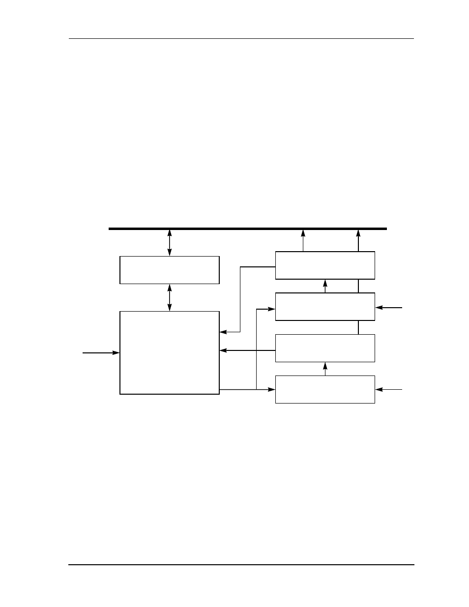
pins are tri-stated. The block diagram of the receiver section is shown in Figure 6-2.
The 24-bit shift registers receive the incoming data from the Serial Data In pins (SDI0
and SDI1, or SDIx). Data is shifted in at the transitions of the serial receive clock
SCKR. Data is assumed to be received MSB first if RDIR is cleared, and LSB first if
RDIR is set. Data is transferred to the SAI receive data registers after 16, 24, or 32 bits
have been shifted in, as determined by the word length control bits RWL1 and
RWL0. A special control mechanism is used to emulate a 32-bit shift register in the
event that the word length is defined as 32 bits. This is done by disabling eight data
shifts at the beginning/end of the data word transfer, according to the RDWT bit in
the RCS register. These shift registers cannot be directly accessed by the DSP.
Figure 6-2 SAI Receive Section Block Diagram
Global Data Bus (GDB)
Rx Control/Status (RCS)
Rx Controller
RCLOCK
0
15
RX0 Shift Register
RX1 Data Register
RX1 Shift Register
SDI1
RX0 Data Register
SDI0
Status
Control
0
23
23
23
23
0
0
0
AA0428
