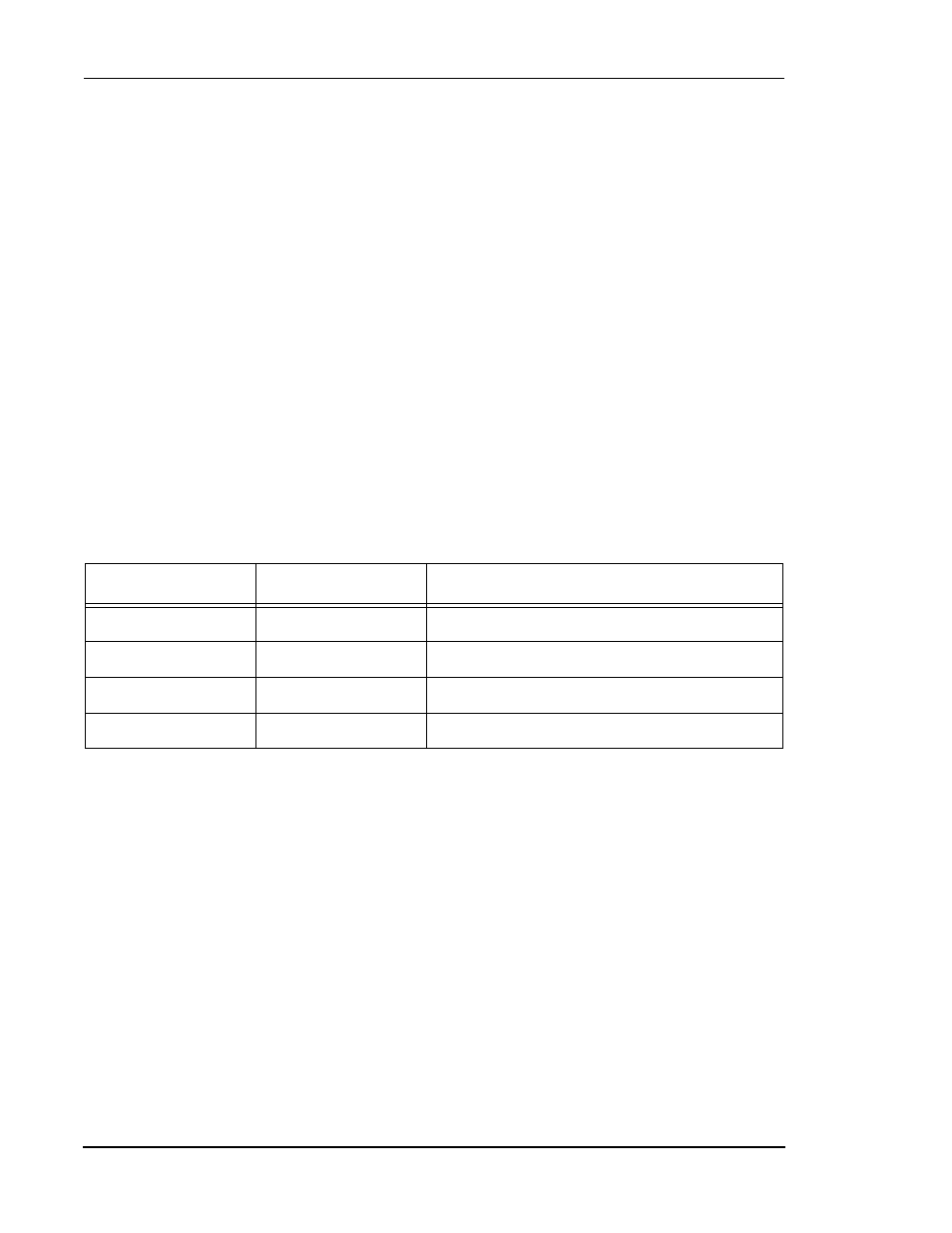
1 gpior data bits (gd[7:0])—bits 7–0, 2 gpior data direction bits (gdd[7:0])—bits 15–8, Table71 gpio pin configuration – Motorola DSP56012 User Manual
Page 208: 3 gpior control bits (gc[7:0])—bits 23–16, Gpior data bits (gd[7:0])—bits 7–0 -4, Gpior data direction bits (gdd[7:0])—bits 15–8 -4, Gpior control bits (gc[7:0])—bits 23–16 -4, Table 7-1, Gpio pin configuration -4

7-4
DSP56012 User’s Manual
MOTOROLA
GPIO
GPIO Register (GPIOR)
7.3.1
GPIOR Data Bits (GD[7:0])—Bits 7–0
The read/write GPIO Data bits (GD[7:0]) are used to read from or write to the
corresponding GPIO[7:0] pins. If the GPIOx pin is defined as an input, the GDx bit
will reflect the logic value present on the GPIOx pin. If the GPIOx pin is defined as an
output, the GPIOx pin will reflect the value written to the GDx bit. The GD[7:0] bits
are cleared during hardware reset and software reset.
7.3.2
GPIOR Data Direction Bits (GDD[7:0])—Bits 15–8
The read/write GPIO Data Direction bits (GDD[7:0]) select the direction of data
transfer for each of the GPIO[7:0] pins (see
). When the GDDx bit is cleared,
the corresponding GPIOx pin is defined as an input. When the GDDx bit is set, the
corresponding GPIOx pin is defined as an output. The GDD[7:0] bits are cleared
during hardware reset and software reset.
7.3.3
GPIOR Control Bits (GC[7:0])—Bits 23–16
The read/write GPIO Control bits (GC[7:0]) select the type of output buffer for each
of the GPIO[7:0] pins when the pins are defined as outputs, and select whether or not
the input buffer is connected to the pin when the pin is defined as an input.
Table 7-1
GPIO Pin Configuration
GDDx
GCx
GPIO Pin Definition
0
0
Disconnected
0
1
Input
1
0
Standard active high/active low output
1
1
Open-drain output
