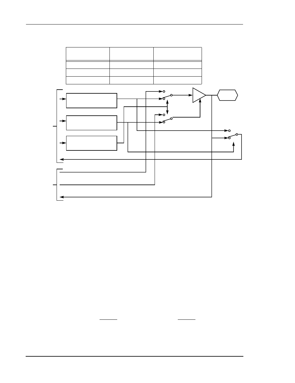
Figure44 port b i/o pin control logic, 1 port b control (pbc) register, Port b control (pbc) register -6 – Motorola DSP56012 User Manual
Page 86: Figure 4-4, Port b i/o pin control logic -6

4-6
DSP56012 User’s Manual
MOTOROLA
Parallel Host Interface
Port B Configuration
4.2.1
Port B Control (PBC) Register
The Port B Control (PBC) register determines which set of functions are used with the
external multiplexed pins. As shown in
on page 4-4, there are three valid
combinations:
• Parallel I/O (default)
• Host Interface
• Host Interface (with HACK as GPIO)
The default setting (BC1:BC0 = 00) defines the pins as GPIO signals. The other
settings must be programmed by writing to the PBC register. Writing a $1 to the
register defines the pins as the HI port. Writing a $2 to the PBC register defines the
pins as an HI port without a HACK signal; the pin used by HACK in the HI is
defined as a GPIO pin (PB14).
Figure 4-4 Port B I/O Pin Control Logic
Port Control
Register Bit
Data Direction
Register Bit
Pin Function
0
0
Port B Input Pin
0
1
Port B Output Pin
1
X
HI Function
Port B
Registers
HI Input Data Bit
HI Data Direction Bit
HI Output Data Bit
Port B Input Data Bit
Pin
Port B Data (PBD)
Register Bit
Data Direction
Register (PBDDR) Bit
Port B Control
Register (PBC) Bit
(GPIO
Position)
(Input
Position)
Peripheral
Logic
AA0310.11
