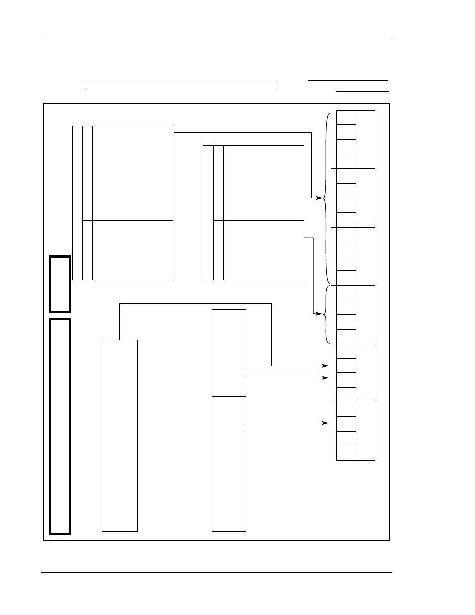
Central processor, Pctl – Motorola DSP56012 User Manual
Page 250

B-18
DSP56012 User’s Manual
MOTOROLA
Programming Reference
Application:
Date:
Programmer:
Sheet 4 of 4
CENTRAL PROCESSOR
1
5
1
4
1
3
1
2
1
1
1
0
987654321
0
DF3
DF2
MF11
MF10
MF7
MF6
MF5
MF4
MF3
MF2
MF1
MF0
PLL Contro
l
X:$FFFD Read/Write
DF1
DF0
Reset = $000002(PINIT = GND)
Register (PCTL)
19
18
17
16
23
22
21
20
*
0
MF8
MF9
PSTP
PEN
CSRC
Multiplication Factor Bits MF0–MF11
MF11–MF0
Multiplication Factor MF
$000
1
$001
2
$002
3
••
••
••
$FFE
4095
$FFF
4096
Stop Processing State Bit (PSTP)
0 = PLL Disabled During Stop Processing State
1 = PLL Enabled During Stop Processing State
PLL Enable Bit (PEN)
0 = Disable PLL
1 = Enable PLL
Chip Clock Source Bit (CSRC)
0 = Output from Low Power Divider
1 = Output from VCO
*
= Reserved, write as 0
*
0
*
0
*
0
*
0
Division Factor Bits DF0–DF11
DF11–DF0
Division Factor MF
$0
2
0
$1
2
1
$2
2
2
••
••
••
$E
2
14
$F
2
15
Reset = $040002(PINIT = Vcc)
PCTL
PLL Control Register (PCTL)
