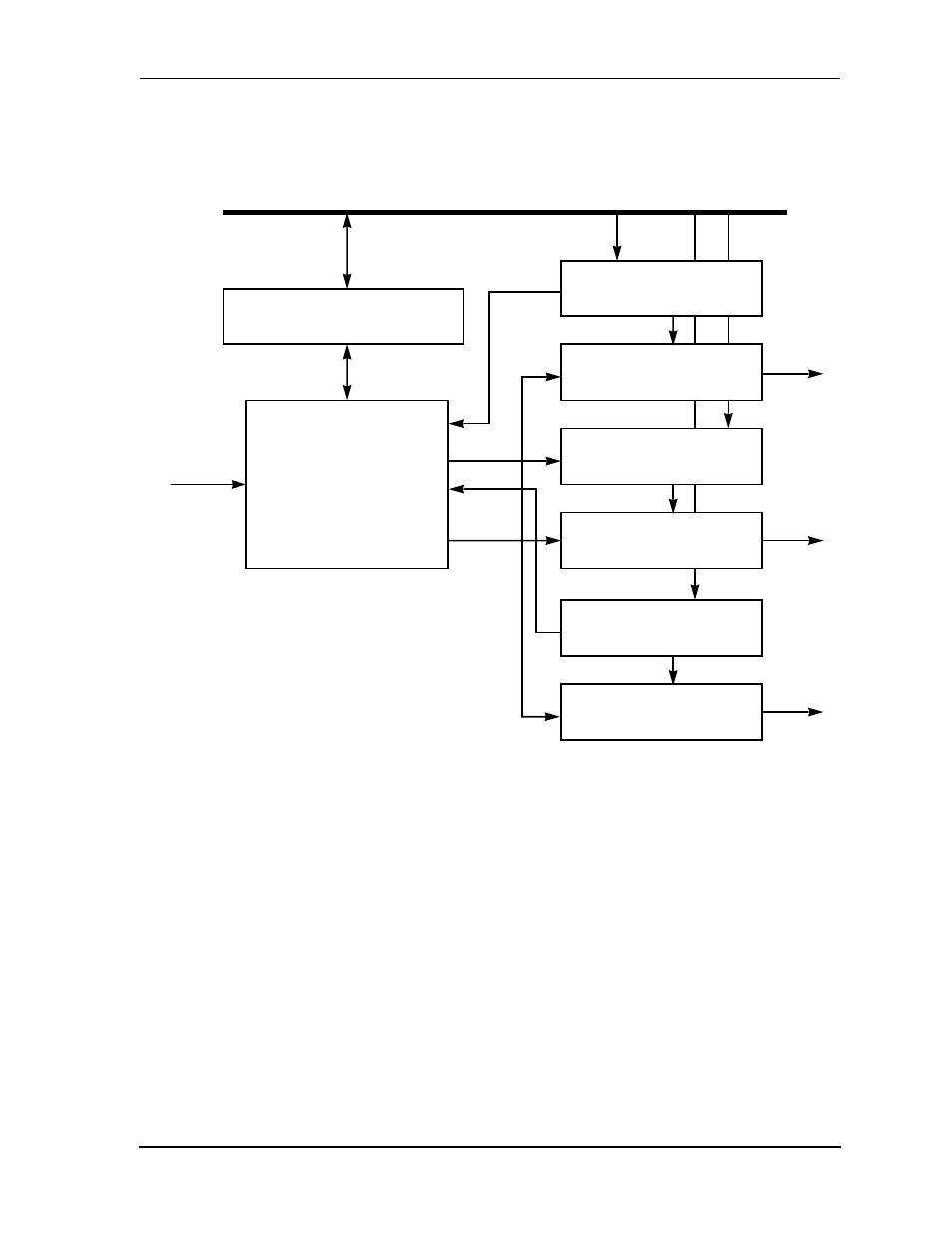
Figure63 sai transmit section block diagram, Figure 6-3, Sai transmit section block diagram -7 – Motorola DSP56012 User Manual
Page 185

Serial Audio Interface
Serial Audio Interface Internal Architecture
MOTOROLA
DSP56012 User’s Manual
6-7
.
The transmitter section data path consists of three fully synchronized sets of data and
shift registers capable of operating simultaneously. In each set, the 24-bit shift
register contains the data being transmitted. Data is shifted out to the associated SDO
pin at the transitions of the serial transmit clock SCKT. Data is shifted out MSB first if
TDIR is cleared, and LSB first if TDIR is set. The number of bits shifted out before the
shift register is considered empty and ready to be reloaded can be 16, 24, or 32 bits as
determined by the TWL1 and TWL0 control bits in the TCS register. A special control
mechanism is used to emulate a 32-bit shift register if the word length is defined as 32
bits. This is done by enabling eight data shifts at the beginning/end of the data word
transfer, according to the TDWE bit in the TCS register. These shift registers cannot
be directly accessed by the DSP.
Figure 6-3 SAI Transmit Section Block Diagram
TX0 Shift Register
Global Data Bus (GDB)
Transmit Control/Status (TCS)
TX1 Data Register
TX1 Shift Register
Transmit Controller
TCLOCK
SDO1
TX0 Data Register
SDO0
Status
Control
0
15
0
23
23
23
23
0
0
0
TX2 Data Register
TX2 Shift Register
SDO2
23
0
23
0
AA0429k
