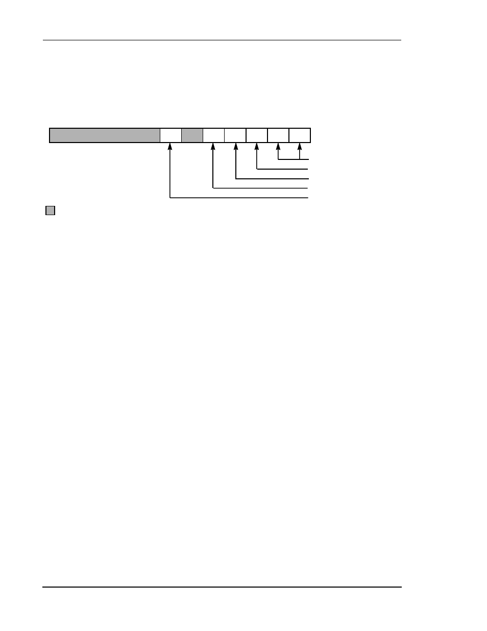
4 operating mode register (omr), Figure35 operating mode register (omr), 1 dsp operating mode (mc, mb, ma)—bits 4, 1, and 0 – Motorola DSP56012 User Manual
Page 72: 3 stop delay (sd)—bit 6, Operating mode register (omr) -12, Stop delay (sd)—bit 6 -12, Figure 3-5, Operating mode register (omr) -11, Program ram enable a (pea)—bit 2 -11

3-12
DSP56012 User’s Manual
MOTOROLA
Memory, Operating Modes, and Interrupts
Operating Mode Register (OMR)
3.4
OPERATING MODE REGISTER (OMR)
The Operating Mode Register (OMR) is illustrated in
3.4.1
DSP Operating Mode (MC, MB, MA)—Bits 4, 1, and 0
The DSP operating mode bits, MC, MB, and MA, select the operating mode of the
DSP56012. These operating modes are described below in
Section
. On hardware reset, MC, MB, and MA are loaded from the external mode
select pins MODC, MODB, and MODA, respectively. After the DSP leaves the reset
state, MC, MB, and MA can be changed under software control.
3.4.2
Program RAM Enable A and Program RAM Enable B (PEA
and PEB)—Bits 2 and 3
The Program RAM Enable A (PEA) and Program RAM Enable B (PEB) bits are used
to alter the memory configuration on the DSP56012. Refer to
for a summary of the memory configurations. The internal memory maps, as selected
by the PEA and PEB bits, are shown in Figure 3-1 through Figure 3-4. PEA and PEB
are cleared by hardware reset.
3.4.3
Stop Delay (SD)—Bit 6
When leaving the Stop state, the Stop Delay (SD) bit is interrogated. If the SD bit is
cleared (SD = 0), a 65,535 core clock cycle delay (131,072 T states) is implemented
before continuation of the STOP instruction cycle. If the SD bit is set (SD = 1), the
delay before continuation of the STOP instruction cycle is set as eight clock cycles (16
Figure 3-5 Operating Mode Register (OMR)
Bits 5 and 7–23 are reserved, read as 0s, and should be written with 0s
MA
MB
PEA
PEB
MC
SD
0
1
2
3
4
5
6
23
7
Operating Mode A,B
Program RAM Enable A
Program RAM Enable B
Operating Mode C
Stop Delay
AA0291k
for future compatibility.
