2 x data memory, 3 y data memory, 4 on-chip memory configuration bits – Motorola DSP56012 User Manual
Page 35: Table14 internal memory configurations, X data memory -15, Y data memory -15, On-chip memory configuration bits -15, Table 1-4, Internal memory configurations -15

Overview
DSP56012 Architectural Overview
MOTOROLA
DSP56012 User’s Manual
1-15
1.3.3.2
X Data Memory
The on-chip X data memory shown in
is 24 bits wide. Addresses are
received from the XAB, and data transfers to the Data ALU occur on the XDB.
1.3.3.3
Y Data Memory
The on-chip Y data memory shown in
is 24 bits wide. Addresses are
received from the YAB, and data transfers to the Data ALU occur on the YDB.
1.3.3.4
On-Chip Memory Configuration Bits
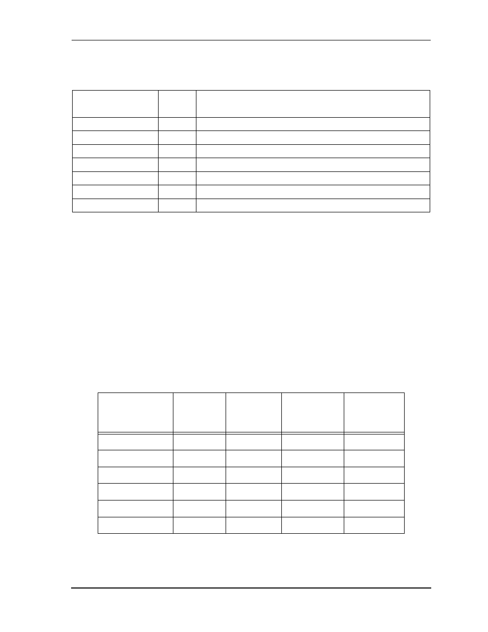
Through the use of bits PEA and PEB in the OMR, four different memory
configurations are possible. These configurations provide appropriate memory sizes
for a variety of applications (see
Section 3
provides detailed information
about memory configuration.
P: $0050
0–2
DAX Transmit Underrun Error
P: $0052
0–2
DAX Block Transferred
P: $0054
Reserved; available for Host Command, see p. B-5–B-6.
P: $0056
0–2
DAX Transmit Register Empty
P: $0058
Reserved; available for Host Command, see p. B-5–B-6.
:
Reserved; available for Host Command, see p. B-5–B-6.
P: $007E
Reserved; available for Host Command, see p. B-5–B-6.
Table 1-4
Internal Memory Configurations
No Switch
(PEA = 0
PEB = 0)
Switch A
(PEA = 1
PEB = 0)
Switch B
(PEA = 0
PEB = 1)
Switch A+B
(PEA = 1
PEB = 1)
Program RAM
0.25 K
1.0 K
1.75 K
2.5 K
X RAM
4.0 K
3.25 K
3.25 K
2.5 K
Y RAM
4.25 K
4.25 K
3.5 K
3.5 K
Program ROM
15 K
15 K
15 K
15 K
X ROM
3.5 K
3.5 K
3.5 K
3.5 K
Y ROM
2.0 K
2.0 K
2.0 K
2.0 K
Table 1-3
Interrupt Starting Addresses and Sources (Continued)
Interrupt
Starting Address
IPL
Interrupt Source
