Maxq610 user’s guide – Maxim Integrated MAXQ610 User Manual
Page 97
6-4
MAXQ610 User’s Guide
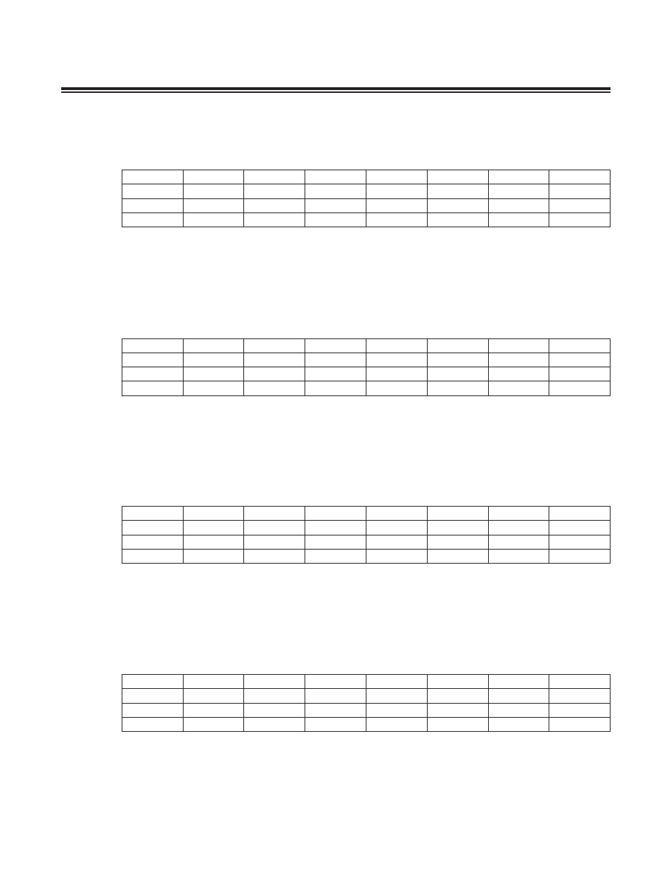
Bits 7:0: Port 2 Output. This register stores the data that is output on any of the pins of port 2 that have been defined
as output pins . If the port pins are in input mode, this register controls the weak pullup enable for each pin . Changing
the data direction of any pins for this port (through register PD2) does not affect the value in this register .
Bits 7:0: Port 3 Output. This register stores the data that is output on any of the pins of port 3 that have been defined
as output pins . If the port pins are in input mode, this register controls the weak pullup enable for each pin . Changing
the data direction of any pins for this port (through register PD3) does not affect the value in this register .
Bits 5:0: Port 4 Output. This register stores the data that is output on any of the pins of port 4 that have been defined
as output pins . If the port pins are in input mode, this register controls the weak pullup enable for each pin . Changing
the data direction of any pins for this port (through register PD4) does not affect the value in this register .
Bits 7:0: Port 0 Input Bits. The read values of these bits reflect the logic states present at port 0 pins P0 .0 to P0 .7 .
Register Name
PO2
Register Description
Port 2 Output Register
Register Address
M0[02h]
Register Name
PO3
Register Description
Port 3 Output Register
Register Address
M0[03h]
Register Name
PO4
Register Description
Port 4 Output Register
Register Address
M1[04h]
Register Name
PI0
Register Description
Port 0 Input Register
Register Address
M0[08h]
Bit #
7
6
5
4
3
2
1
0
Name
PO2 .7
PO2 .6
PO2 .5
PO2 .4
PO2 .3
PO2 .2
PO2 .1
PO2 .0
Reset
s
s
s
s
s
s
s
s
Access
rw
rw
rw
rw
rw
rw
rw
rw
Bit #
7
6
5
4
3
2
1
0
Name
PO3 .7
PO3 .6
PO3 .5
PO3 .4
PO3 .3
PO3 .2
PO3 .1
PO3 .0
Reset
s
s
s
s
s
s
s
s
Access
rw
rw
rw
rw
rw
rw
rw
rw
Bit #
7
6
5
4
3
2
1
0
Name
—
—
PO4 .5
PO4 .4
PO4 .3
PO4 .2
PO4 .1
PO4 .0
Reset
0
0
s
s
s
s
s
s
Access
r
r
rw
rw
rw
rw
rw
rw
Bit #
7
6
5
4
3
2
1
0
Name
PI0 .7
PI0 .6
PI0 .5
PI0 .4
PI0 .3
PI0 .2
PI0 .1
PI0 .0
Reset
s
s
s
s
s
s
s
s
Access
r
r
r
r
r
r
r
r