1 spi transfer formats, 10 .1 spi transfer formats -2, Figure 10-1 . spi block diagram -2 – Maxim Integrated MAXQ610 User Manual
Page 138: Table 10-1 . spi module signal functions -2, Maxq610 user’s guide, Table 10-1. spi module signal functions
10-2
MAXQ610 User’s Guide
SECTION 10: SERIAL PERIPHERAL INTERFACE (SPI) MODULE
The serial peripheral interface (SPI) module of the MAXQ610 microcontroller provides an independent serial commu-
nication channel to communicate synchronously with peripheral devices in a multiple master or multiple slave system .
The interface allows access to a 4-wire full-duplex serial bus that can be operated in either master mode or slave
mode . The SPI functionality must be enabled by setting the SPI enable (SPIEN) bit of the SPI control register to 1 . The
maximum data rate of the SPI interface is 1/2 the system clock frequency for master mode operation and 1/4 the system
clock frequency for slave mode operation .
The four external interface signals used by the SPI module are MISO, MOSI, SPICK, and SSEL . Table 10-1 shows the
function of each of these signals .
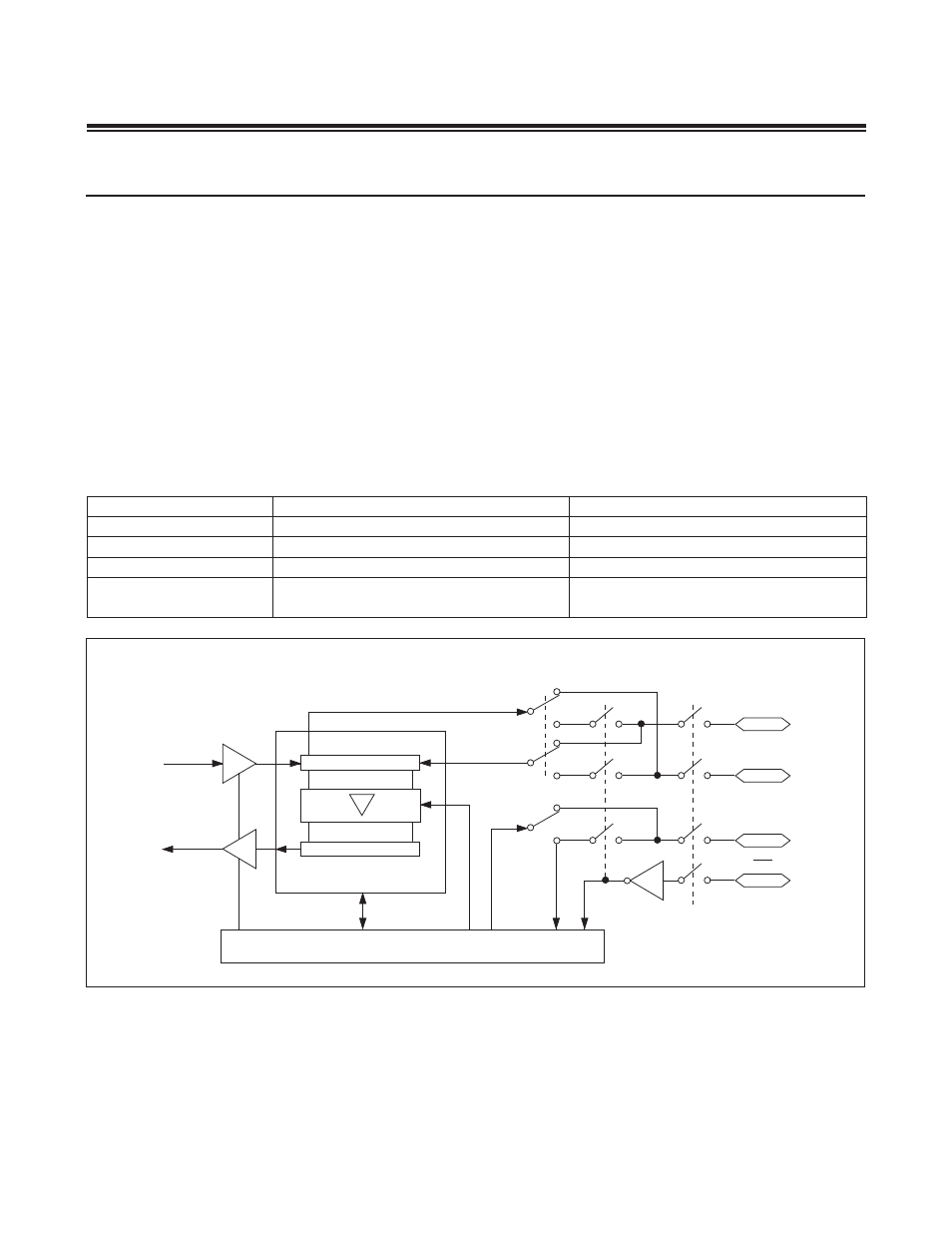
Figure 10-1 shows the SPI external interface signals, control unit, read buffer, and single shift register common to the
transmit and receive data path . Each time that an SPI transfer completes, the received character is transferred to the
read buffer, giving double buffering on the receive side . The CPU has read/write access to the control unit and the SPI
data buffer (SPIB) . Writes to SPIB are always directed to the shift register while reads always come from the receive
holding buffer .
10.1 SPI Transfer Formats
During an SPI transfer, data is simultaneously transmitted and received over two serial data lines with respect to a sin-
gle serial shift clock . The polarity and phase of the serial shift clock are the primary components in defining the SPI data
Table 10-1. SPI Module Signal Functions
Figure 10-1. SPI Block Diagram
SPIEN =
SPICN.0
MSTM = SPICN.1
SHIFT REGISTER
MOSI
SPIB WRITES
RECEIVE DATA
BUFFER
SPIB READS
0
0
1
15/7
15/7
MISO
0
1
SPI STATUS AND CONTROL UNIT
0
SPICK
1
0
SSEL
EXTERNAL PIN SIGNAL
MASTER MODE USE
SLAVE MODE USE
MISO: Master In/Slave Out
Input to serial shift register
Output from serial shift register when selected
MOSI: Master Out/Slave In
Output from serial shift register
Input to serial shift register when selected
SPICK: SPI Clock
Serial shift clock sourced to slave device(s)
Serial shift clock from an external master
SSEL: Slave Select
(Optional) Mode fault-detection input if enabled
(MODFE = 1)
Slave-select input