Maxq610 user’s guide – Maxim Integrated MAXQ610 User Manual
Page 139
10-3
MAXQ610 User’s Guide
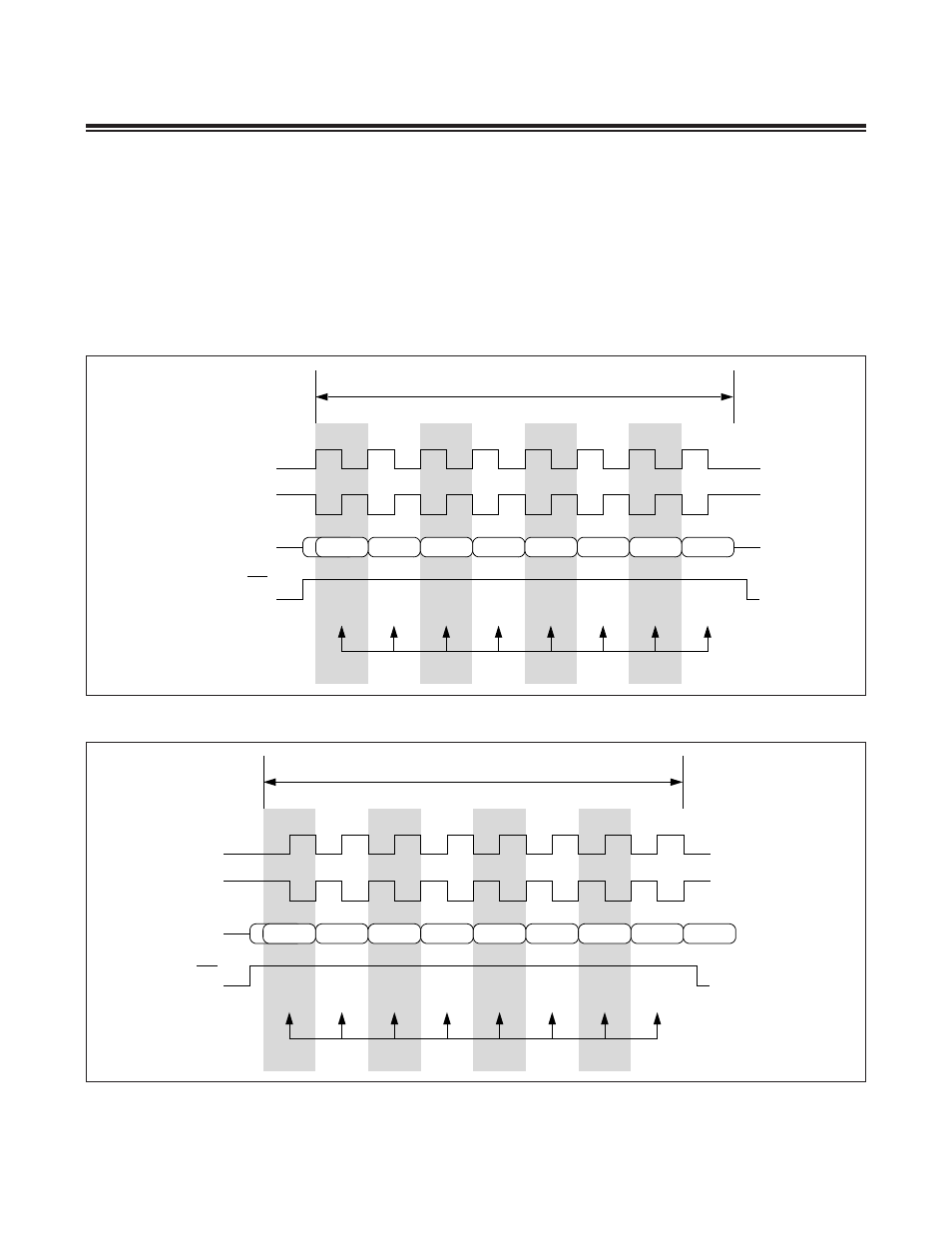
transfer format . The polarity of the serial clock corresponds to the idle logic state of the clock line and therefore also
defines which clock edge is the active edge . To define a serial shift clock signal that idles in a logic-low state (active
clock edge = rising), the clock polarity select bit (CKPOL; SPICF .0) should be configured to a 0, while setting CKPOL
= 1 causes the shift clock to idle in a logic-high state (active clock edge = falling) . The phase of the serial clock selects
which edge is used to sample the serial shift data . The clock phase select bit (CKPHA; SPICF .1) controls whether the
active or inactive clock edge is used to latch the data . When CKPHA is set to 1, data is sampled on the inactive clock
edge (clock returning to the idle state) . When CKPHA is set to 0, data is sampled on the active clock edge (clock
transition to the active state) . Together, the CKPOL and CKPHA bits allow the four possible SPI data transfer formats
illustrated in Figure 10-2 and Figure 10-3 . The SSEL signal can remain asserted between successive transfers .
Figure 10-2. SPI Transfer Formats (CKPHA = 1)
Figure 10-3. SPI Transfer Formats (CKPHA = 0)
TRANSFER CYCLE
CKPHA = 1
CKPHA = 1
SSEL
MSB
LSB
1
2
3
4
5
6
7
8
SAS = 1
SAMPLING POINTS
CKPOL = 0
MOSI/MISO
CKPOL = 1
TRANSFER CYCLE
CKPHA = 0
CKPHA = 0
SSEL
MSB
MSB
MSB OF
NEXT TRANSFER
LSB
1
2
3
4
5
6
7
8
SAS = 1
SAMPLING POINTS
CKPOL = 0
MOSI/MISO
CKPOL = 1