1 external clock (crystal/resonator), 2 external clock (direct input), Figure 2-10 . on-chip crystal oscillator -23 – Maxim Integrated MAXQ610 User Manual
Page 27: Maxq610 user’s guide
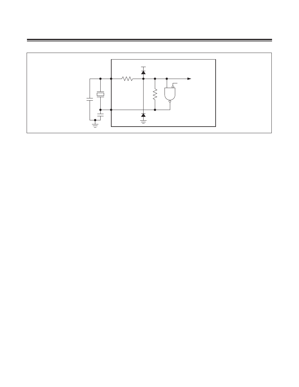
2-23
MAXQ610 User’s Guide
2.7.1 External Clock (Crystal/Resonator)
An external quartz crystal or a ceramic resonator can be connected from HFXIN to HFXOUT determining the frequency,
as illustrated in Figure 2-10. The fundamental mode of the crystal operates as inductive reactance in parallel resonance
with external capacitance to the crystal.
Crystal specifications, operating temperature, operating voltage, and parasitic capacitance must be considered when
designing the internal oscillator. The MAXQ610 is designed to operate at a 12MHz maximum frequency. To further
reduce the effects of external noise, a guard ring can be placed around the oscillator circuitry.
Pins HFXIN and HFXOUT are protected by clamping devices against on-chip electrostatic discharge. These clamping
devices are diodes parasitic to the feedback resistor R
F
in the oscillator’s inverter circuit. The inverter circuit is pre-
sented as a NAND gate that can disable clock generation in stop mode.
Noise at HFXIN and HFXOUT can adversely affect on-chip clock timing. It is good design practice to place the crystal
and capacitors near the oscillator circuitry and connect to HFXIN, HFXOUT, and ground with a direct shot trace. The
typical values of external capacitors vary with the type of crystal used and should be initially selected based on the
load capacitance as suggested by the crystal manufacturer.
For cost-sensitive applications, a ceramic resonator can be used instead of a crystal. Using the ceramic resonator can
require a different circuit configuration and capacitance value.
2.7.2 External Clock (Direct Input)
The MAXQ610 CPU can also obtain the system clock signal directly from an external clock source. In this configuration,
the clock generation circuitry is driven directly by an external clock.
To operate the MAXQ610 from an external clock, connect the clock source to HFXIN and leave HFXOUT unconnected.
The clock source should be driven through a CMOS driver. If the clock driver is a TTL gate, its output must be con-
nected to V
DD
through a pullup resistor to ensure a satisfactory logic level for active clock pulses. To minimize system
noise on the clock circuitry, the external clock source must meet the maximum rise and fall times and the minimum high
and low times specified for the clock source. The external noise can affect clock generation circuit if these parameters
do not meet the specification.
Figure 2-10. On-Chip Crystal Oscillator
MAXQ610
V
DD
STOP
CLOCK CIRCUIT
R
F
C2
C1
HFXIN
HFXOUT
RF = 1M
Ω ± 50%
C1 = C2 = 30pF