Table 3.12 scsi channel [1] control signals, 5 memory interface, Table 3.13 flash rom/nvsram interface pins (cont.) – Avago Technologies LSI53C1030 User Manual
Page 74: Memory interface, Flash rom/nvsram interface pins, Section 3.5, “memory interface
3-14
Signal Description
Version 2.2
Copyright © 2001, 2002, 2003 by LSI Logic Corporation. All rights reserved.
describes the SCSI Channel [1] Control signals.
3.5 Memory Interface
describes the Flash ROM/NVSRAM Interface signals.
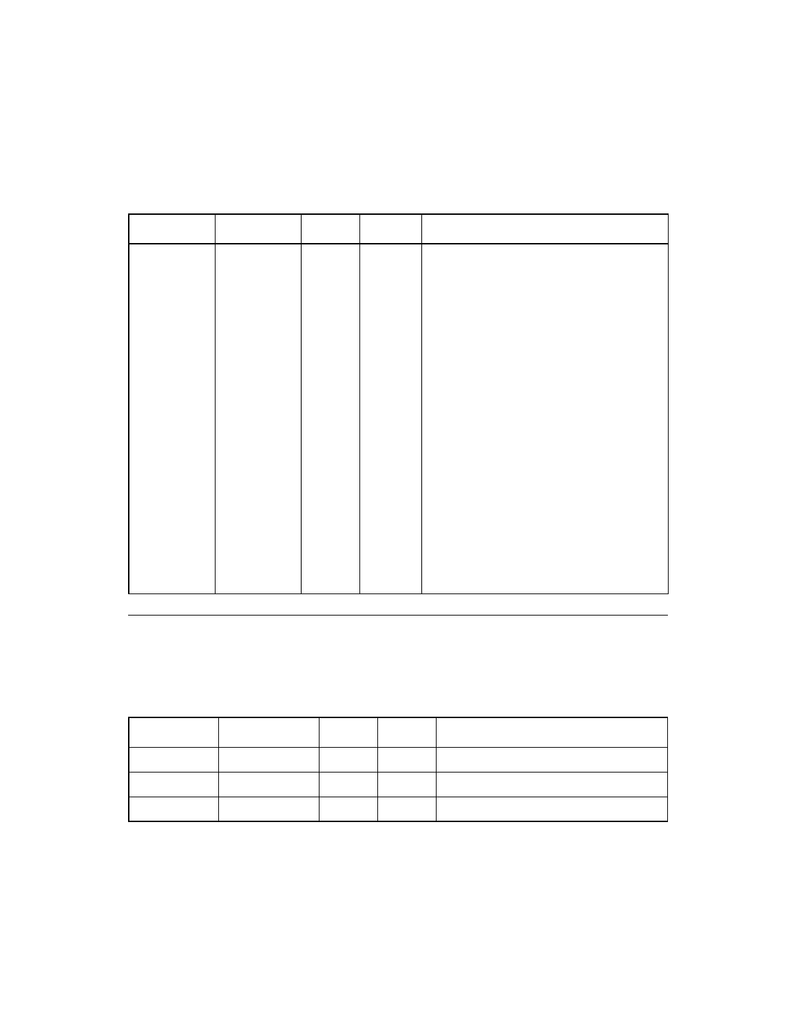
Table 3.12
SCSI Channel [1] Control Signals
Signal Name
BGA Position
Type
Strength
Description
B_SCD-
B_SCD+
B_SIO-
B_SIO+
B_SMSG-
B_SMSG+
B_SREQ-
B_SREQ+
B_SACK-
B_SACK+
B_SBSY-
B_SBSY+
B_SATN-
B_SATN+
B_SRST-
B_SRST+
B_SSEL-
B_SSEL+
E16
D17
E17
D18
B16
D16
B18
C18
D14
E14
A15
B15
B14
D13
E15
A16
B17
C17
I/O
SE:
48 mA
LVD:
12 mA
SCSI Channel [1] Command/Data.
SCSI Channel [1] Input/Output.
SCSI Channel [1] Message.
SCSI Channel [1] Request.
SCSI Channel [1] Acknowledge.
SCSI Channel [1] Busy.
SCSI Channel [1] Attention.
SCSI Channel [1] Bus Reset.
SCSI Channel [1] Select.
Table 3.13
Flash ROM/NVSRAM Interface Pins
Signal Name
BGA Position
Type
Strength Description
MCLK
E20
O
4 mA
Reserved.
ADSC/
D21
O
4 mA
Reserved.
ADV/
B23
O
4 mA
Reserved.