Message upper address, Message data, Register: 0xxx – Avago Technologies LSI53C1030 User Manual
Page 109
PCI Configuration Space Register Description
4-23
Version 2.2
Copyright © 2001, 2002, 2003 by LSI Logic Corporation. All rights reserved.
Message Address
[31:2]
This register contains message address bits [31:2] for the
MSI memory write transaction. The host system specifies
and Dword aligns the message address. During the
address phase, the LSI53C1030 drives Message
Address[1:0] to 0b00.
Reserved
[1:0]
This field is reserved.
Register: 0xXX
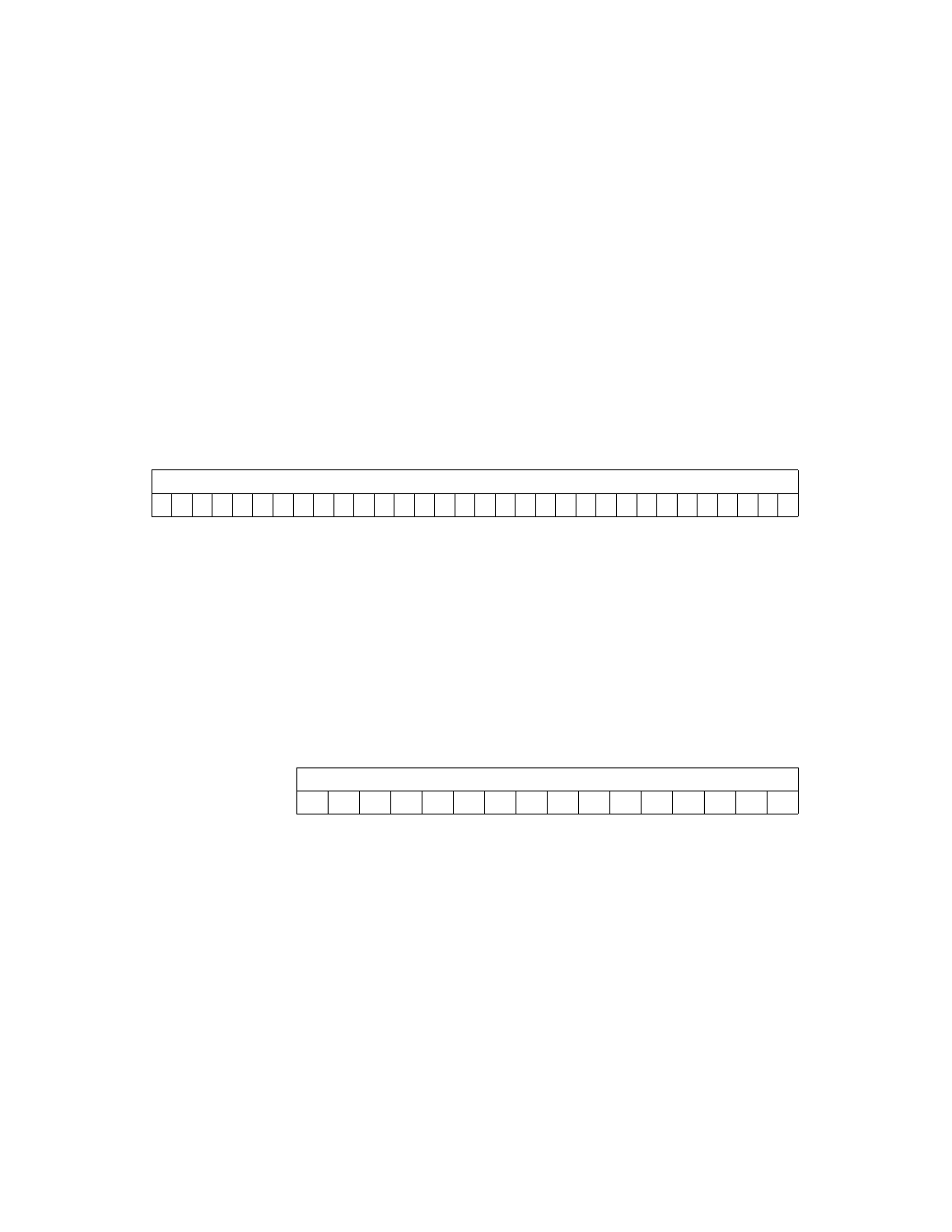
Message Upper Address
Read/Write
Message Upper Address
[31:0]
The LSI53C1030 supports 64-bit MSI. This register con-
tains the upper 32 bits of the 64-bit message address,
which the system specifies. The host system software
can program this register to 0x0000 to force the PCI func-
tion to generate 32-bit message addresses.
Register: 0xXX
Message Data
Read/Write
Message Data
[15:0]
System software initializes this register by writing to it.
The LSI53C1030 sends an interrupt message by writing
a Dword to the address held in the
and
registers. This register forms
bits [15:0] of the Dword message that the PCI function
passes to the host. The PCI function drives bits [31:16]
of this message to 0x0000.
31
0
Message Upper Address
0
0
0
0
0
0
0
0
0
0
0
0
0
0
0
0
0
0
0
0
0
0
0
0
0
0
0
0
0
0
0
0
15
0
Message Data
0
0
0
0
0
0
0
0
0
0
0
0
0
0
0
0