Figure2.5 nvsram diagram, 6 serial eeprom interface, Serial eeprom interface – Avago Technologies LSI53C1030 User Manual
Page 57: Nvsram diagram, Section 2.6, “serial eeprom interface, Section 2.6, “serial eeprom, Interface
Serial EEPROM Interface
2-27
Version 2.2
Copyright © 2001, 2002, 2003 by LSI Logic Corporation. All rights reserved.
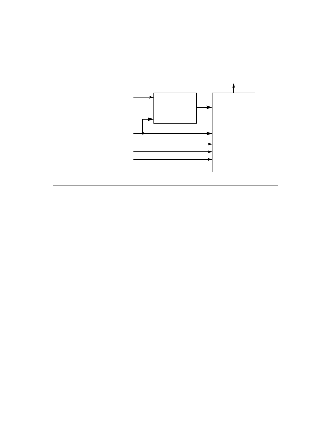
Figure 2.5
NVSRAM Diagram
2.6 Serial EEPROM Interface
The nonvolatile external serial EEPROM stores configuration fields for
the LSI53C1030. The serial EEPROM contains fields for the Subsystem
ID(s), Subsystem Vendor ID(s), and the size of the PCI Diagnostic
Memory Space. The LSI53C1030 must establish each of these
parameters prior to reading system BIOS and loading the PCI
Configuration Space registers. The power-on option settings enable the
download of PCI configuration data from the serial EEPROM. For more
information on the setting of the power-on options, refer to
“Power-On Sense Pins Description.”
A 2-wire serial interface provides the connection to the serial EEPROM.
During initialization, the firmware checks if a serial EEPROM exists.
Firmware uses the checksum byte to determine if the configuration held
in the serial EEPROM is valid. If the checksum fails the firmware checks
for a valid NVData signature. If a valid NVData signature is found the
firmware individually checksums each persistent configuration page to
find the invalid page or pages.
provides the structure of the
configuration record in the serial EEPROM.
FLSHALE[1:0]/
MAD[7:0]
MAS[1:0]
MAD[7:0]
MAD[14:0]
A[14:0]
D[7:0]
RAMCE/
MOE/
BWE[0]/
CE/
OE/
WE/
NVSRAM (32 K x 8)
3.3 V
CPLD
CY37032