2 scsi channel [1] signals, Table 3.11 scsi channel [1] interface signals, Scsi channel [1] signals – Avago Technologies LSI53C1030 User Manual
Page 73: Scsi channel [1] interface signals
SCSI Interface Signals
3-13
Version 2.2
Copyright © 2001, 2002, 2003 by LSI Logic Corporation. All rights reserved.
3.4.2 SCSI Channel [1] Signals
describes the SCSI Channel [1] Interface signals.
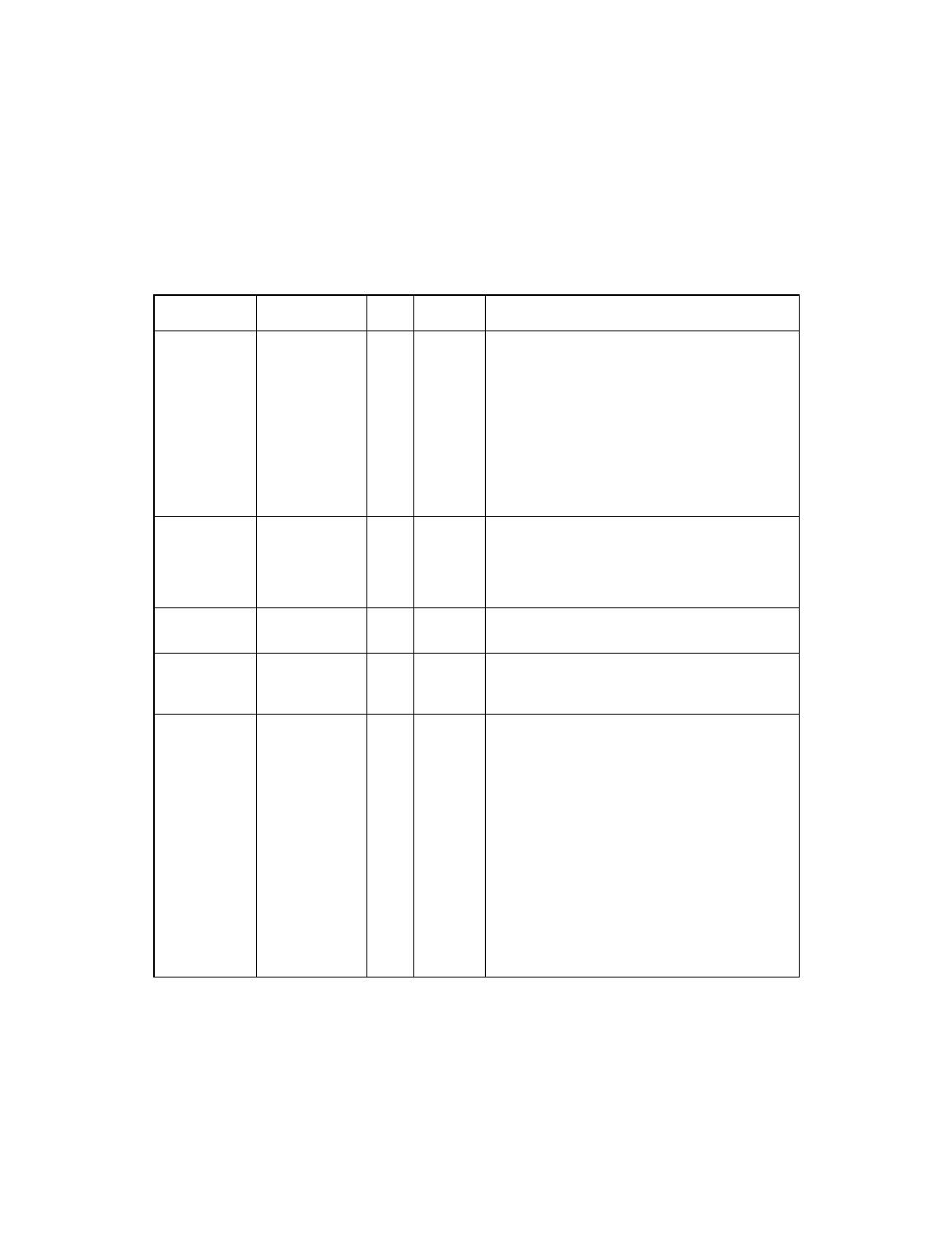
Table 3.11
SCSI Channel [1] Interface Signals
Signal Name
BGA Position
Type
Strength
Description
B_SD[15:0]-
B_SD[15:0]+
D8, E8, C6, A3,
B21, D19, E18,
A19, E13, A12,
B11, B10, D10,
C9, D9, B8
B7, B6, B5, A4,
A23, B20, A20,
B19, E12, B12,
D11, C10, E11,
E10, B9, A8
I/O
SE:
48 mA
LVD:
12 mA
SCSI Channel [1] Data signals.
B_SDP[1:0]-
B_SDP[1:0]+
A7, D12
E9, C13
I/O
SE:
48 mA
LVD:
12 mA
SCSI Channel [1] Data Parity signals.
B_VDDBIAS
B13
O
N/A
B_VDDBIAS provides power for the B_RBIAS
circuit.
B_RBIAS
A11
I
N/A
Connect a 9.76 k
Ω
or 10.0 k
Ω
resistor between
the B_VVDBIAS and B_RBIAS pins to generate
the LVD signalling pad bias current.
B_DIFFSENS
B22
I
N/A
The SCSI Channel [1] Differential Sense pin
detects the present mode of the SCSI bus. This
signal is 5 V tolerant and must connect to the
DIFFSENS signal on the physical SCSI bus.
SE Mode: Driving this pin below 0.5 V (low)
indicates an SE bus and places SCSI
Channel [1] in the SE mode.
LVD Mode: Driving this signal between 0.7 V
and 1.9 V (intermediate) indicates an LVD bus
and places SCSI Channel [1] in the LVD mode.
HVD Mode: Driving this pin above 2.0 V (high)
indicates an HVD bus and causes SCSI
Channel [1] to 3-state its SCSI drivers.