Diagnostic read/write data, Test base address, Diagnostic read/write – Avago Technologies LSI53C1030 User Manual
Page 119: Data, Diagnostic, Read/write data, Register: 0x0c, Register: 0x10
PCI I/O Space and Memory Space Register Description
4-33
Version 2.2
Copyright © 2001, 2002, 2003 by LSI Logic Corporation. All rights reserved.
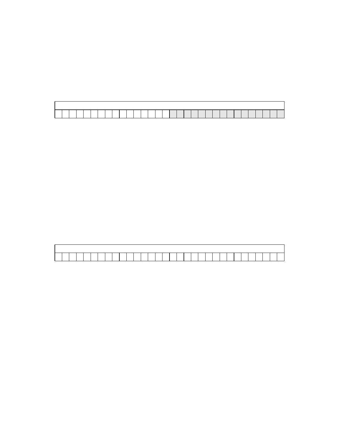
Register: 0x0C
Test Base Address
Read/Write
The Test Base Address register specifies the base address for Memory
Space [1] accesses. There is one Test Base Address register that is
visible to both PCI functions. The two PCI functions physically share this
register. Because Diagnostic Memory is visible only to PCI Function [0],
PCI Function [1] cannot write to this register.
Test Base Address
[31:16]
The number of significant bits is determined by the size
of the PCI Memory Space [1] in the serial EEPROM.
Reserved
[15:0]
This field is reserved.
Register: 0x10
Diagnostic Read/Write Data
Read/Write
This register reads or writes Dword locations on the LSI53C1030 internal
bus. This register is only accessible through PCI I/O Space and returns
0xFFFFFFFF if read through PCI Memory Space. The host can enable
write access to this register by writing the correct Write I/O Key to the
register and setting bit 4, the Diagnostic Write Enable
bit, of the
register. A write of any value other than the
correct Write I/O Key to the
register disables write
access to this register. There is one
register
that is visible to both PCI functions. The two PCI functions physically
share this register.
31
16 15
0
Test Base Address
0
0
0
0
0
0
0
0
0
0
0
0
0
0
0
0
0
0
0
0
0
0
0
0
0
0
0
0
0
0
0
0
31
0
Diagnostic Read/Write Data
0
0
0
0
0
0
0
0
0
0
0
0
0
0
0
0
0
0
0
0
0
0
0
0
0
0
0
0
0
0
0
0