Table 5.1 absolute maximum stress ratings, Table 5.2 operating conditions, Absolute maximum stress ratings – Avago Technologies LSI53C1030 User Manual
Page 126: Operating conditions
5-2
Specifications
Version 2.2
Copyright © 2001, 2002, 2003 by LSI Logic Corporation. All rights reserved.
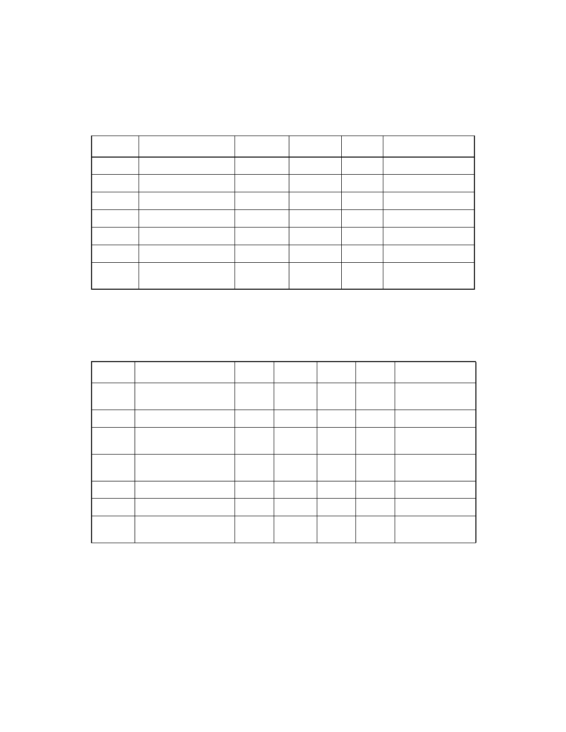
Table 5.1
Absolute Maximum Stress Ratings
1
1. Stresses beyond those listed above can damage the device. These are stress ratings only; func-
tional operation of the device at or beyond these values is not implied.
Symbol
Parameter
Min
Max
Unit
Test Conditions
T
STG
Storage temperature
−
40
125
°
C
–
V
DD-Core
Supply voltage
−
0.3
2.2
V
–
V
DD-IO
I/O Supply voltage
−
0.3
3.9
V
–
V
IN
Input voltage
−
0.5
V
DD
+ 0.5
V
–
I
LP
2
Latch-up current
±
150
–
mA
−
2 V < V
PIN
< 8 V
T
2
Lead temperature
–
125
°
C
–
ESD
2
2. SCSI pins only.
Electrostatic discharge
–
2000
V
MIL-STD 883C,
Method 3015.7
Table 5.2
Operating Conditions
1
1. Conditions that exceed the operating limits can cause the device to function incorrectly.
Symbol
Parameter
Min
Nominal
Max
Unit
Test Conditions
V
DD-Core
Core and analog supply
voltage
1.71
1.80
1.89
V
–
V
DD-IO
I/O supply voltage
2.97
3.30
3.63
V
–
I
DD-Core
Core and analog supply
current (dynamic)
2
2. Core and analog supply only.
–
1.50
1.80
A
–
I
DD-I/O
I/O supply current
(dynamic)
–
0.50
1.00
A
–
T
j
Junction temperature
–
–
115
°
C
–
T
A
Operating free air
0
–
70.0
°
C
–
θ
JA
Thermal resistance
(junction to ambient air)
–
–
15.0
°
C/W
0 Linear
Feet/Minute