Figure5.2 lvd receiver, Table 5.5 a_diffsens and b_diffsens scsi signals, Table 5.6 input capacitance – Avago Technologies LSI53C1030 User Manual
Page 128: Lvd receiver, A_diffsens and b_diffsens scsi signals, Input capacitance
5-4
Specifications
Version 2.2
Copyright © 2001, 2002, 2003 by LSI Logic Corporation. All rights reserved.
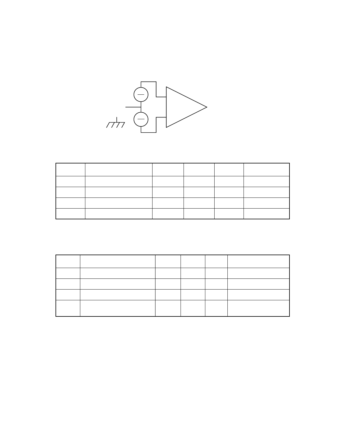
Figure 5.2
LVD Receiver
V
CM
+
−
+
+
+
−
−
−
V
I
2
V
I
2
Table 5.5
A_DIFFSENS and B_DIFFSENS SCSI Signals
Symbol
Parameter
Min
Max
Unit
Test Conditions
V
IH
HVD sense voltage
2.4
3.6
V
Note 1
V
S
LVD sense voltage
0.7
1.9
V
Note 1
V
IL
SE sense voltage
V
SS
−
0.35
0.5
V
Note 1
I
OZ
3-state leakage
−
10
10
µ
A
V
PIN
= 0 V, 3.6 V
1. V
IH
, V
IL
, and V
s
are specified in the SPI-4 draft specification.
Table 5.6
Input Capacitance
Symbol
Parameter
Min
Max
Unit
Test Conditions
C
I
Input capacitance of input pads
–
7
pF
Guaranteed by design
C
IO
Input capacitance of I/O pads
–
15
pF
Guaranteed by design
C
PCI
Input capacitance of PCI pads
–
8
pF
Guaranteed by design
C
LVD
Input capacitance of LVD pads
–
8
pF
6.5 pF pad
1.5 pF package
See also other documents in the category Avago Technologies Hardware:
- MGA-725M4 (4 pages)
- MGA-71543 (4 pages)
- MGA-71543 (3 pages)
- MGA-82563 (6 pages)
- 3ware SAS 9750-8i (48 pages)
- 3ware 9690SA-8I (Channel) (138 pages)
- 3ware 9690SA-8I (Channel) (380 pages)
- 3ware SAS 9750-8i (29 pages)
- 3ware 9550SXU-8LP (Channel) (149 pages)
- 3ware 9550SXU-8LP (Channel) (40 pages)
- 3ware 9650SE-8LPML (Channel) (45 pages)
- 3ware 9690SA-8I (Channel) (27 pages)
- 3ware 9690SA-8I (Channel) (361 pages)
- 6160 SAS Switch (2 pages)
- Cache Protection for RAID Controller Cards (13 pages)
- MegaRAID SAS 9271-8iCC (13 pages)
- MegaRAID SAS 9361-8i (13 pages)
- MegaRAID SAS 9266-8i (12 pages)
- MegaRAID SAS 9380-8e (43 pages)
- Cache Protection for RAID Controller Cards (139 pages)
- MegaRAID SafeStore Software (502 pages)
- MegaRAID SAS 9285-8ecv (80 pages)
- MegaRAID SAS 9285-8ecv (92 pages)
- MegaRAID SAS 9266-8i (20 pages)
- MegaRAID SAS 9271-8iCC (26 pages)
- MegaRAID SAS 9271-8i (8 pages)
- MegaRAID SAS 0260CV-4i (72 pages)
- MegaRAID SAS 0260CV-4i (64 pages)
- MegaRAID SAS 0260CV-4i (49 pages)
- MegaRAID SAS 9361-8i (7 pages)
- MegaRAID SAS 9341-8i (8 pages)
- MegaRAID SAS 9380-4i4e (7 pages)
- MegaRAID SAS 9380-8e (7 pages)
- MegaRAID SAS 0260CV-4i (28 pages)
- MegaRAID SAS 9240-8i (4 pages)
- MegaRAID SAS 9280-24i4e (14 pages)
- MegaRAID SAS 9280-24i4e (16 pages)
- MegaRAID SAS 9260-16i (12 pages)
- MegaRAID SAS 9280-8e (22 pages)
- MegaRAID SAS 9260-8i (4 pages)
- MegaRAID SafeStore Software (8 pages)
- MegaRAID SAS 9261-8i (4 pages)
- MegaRAID SAS 9285-8e (12 pages)
- MegaRAID SAS 9280-16i4e (12 pages)
- MegaRAID SAS 9280-4i4e (4 pages)