Figure5.7 interrupt output, 4 external memory timing diagrams, 1 nvsram timing – Avago Technologies LSI53C1030 User Manual
Page 135: Table 5.16 nvsram read cycle timing, External memory timing diagrams, Nvsram timing, Interrupt output, Nvsram read cycle timing, Section 5.4, “external memory timing diagrams, Figure 5.7
External Memory Timing Diagrams
5-11
Version 2.2
Copyright © 2001, 2002, 2003 by LSI Logic Corporation. All rights reserved.
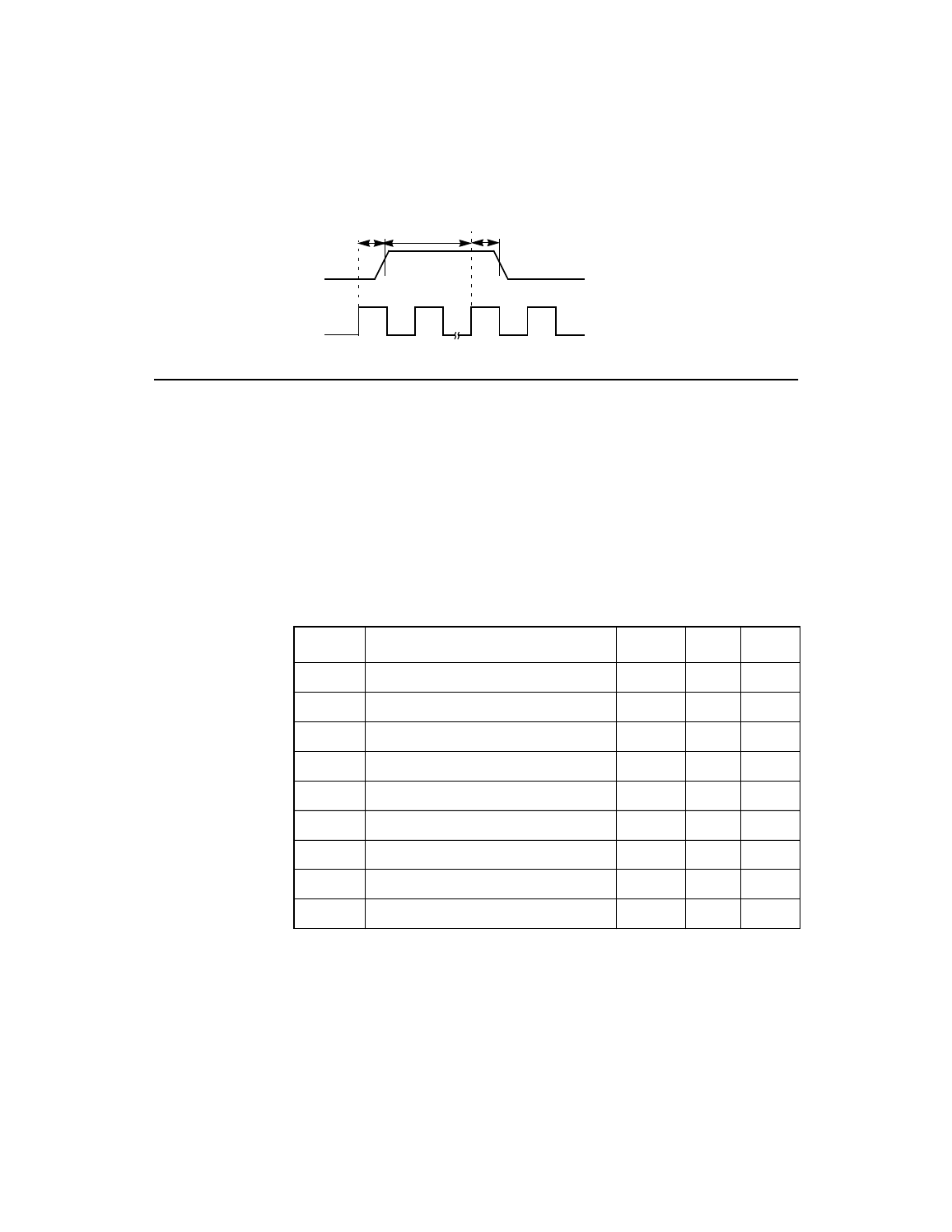
Figure 5.7
Interrupt Output
5.4 External Memory Timing Diagrams
This section provides timing diagrams and data for NVSRAM and Flash
ROM timings.
5.4.1 NVSRAM Timing
and
provide the timing information for the Memory
Address and Data (MAD) bus NVSRAM read accesses.
t
1
t
2
t
3
IRQ/
CLK
Table 5.16
NVSRAM Read Cycle Timing
Symbol
Parameter
Min
Max
Unit
t
1
Address setup to FLSHALE/ HIGH
25
–
ns
t
2
Address hold from FLSHALE/ HIGH
25
–
ns
t
3
FLSHALE/ pulse width
25
–
ns
t
4
Address valid to data clocked in
135
–
ns
t
5
RAMCE/ LOW to data clocked in
85
–
ns
t
6
MOE/ LOW to data clocked in
75
–
ns
t
7
Data setup to MOE/ HIGH
10
–
ns
t
8
Data setup to RAMCE/ HIGH
10
–
ns
t
9
Data hold from RAMCE/ HIGH
0
–
ns
- MGA-725M4 (4 pages)
- MGA-71543 (4 pages)
- MGA-71543 (3 pages)
- MGA-82563 (6 pages)
- 3ware 9690SA-8I (Channel) (138 pages)
- 3ware 9690SA-8I (Channel) (380 pages)
- 3ware SAS 9750-8i (48 pages)
- 3ware SAS 9750-8i (29 pages)
- 3ware 9550SXU-8LP (Channel) (149 pages)
- 3ware 9550SXU-8LP (Channel) (40 pages)
- 3ware 9650SE-8LPML (Channel) (45 pages)
- 3ware 9690SA-8I (Channel) (27 pages)
- 3ware 9690SA-8I (Channel) (361 pages)
- 6160 SAS Switch (2 pages)
- MegaRAID SAS 9361-8i (13 pages)
- MegaRAID SAS 9266-8i (12 pages)
- MegaRAID SAS 9380-8e (43 pages)
- Cache Protection for RAID Controller Cards (139 pages)
- Cache Protection for RAID Controller Cards (13 pages)
- MegaRAID SAS 9271-8iCC (13 pages)
- MegaRAID SAS 9285-8ecv (92 pages)
- MegaRAID SAS 9266-8i (20 pages)
- MegaRAID SAS 9271-8iCC (26 pages)
- MegaRAID SafeStore Software (502 pages)
- MegaRAID SAS 9285-8ecv (80 pages)
- MegaRAID SAS 0260CV-4i (64 pages)
- MegaRAID SAS 0260CV-4i (49 pages)
- MegaRAID SAS 9271-8i (8 pages)
- MegaRAID SAS 0260CV-4i (72 pages)
- MegaRAID SAS 9361-8i (7 pages)
- MegaRAID SAS 9341-8i (8 pages)
- MegaRAID SAS 9380-4i4e (7 pages)
- MegaRAID SAS 9380-8e (7 pages)
- MegaRAID SAS 9240-8i (4 pages)
- MegaRAID SAS 0260CV-4i (28 pages)
- MegaRAID SAS 9260-16i (12 pages)
- MegaRAID SAS 9280-24i4e (14 pages)
- MegaRAID SAS 9280-24i4e (16 pages)
- MegaRAID SAS 9260-8i (4 pages)
- MegaRAID SafeStore Software (8 pages)
- MegaRAID SAS 9280-8e (22 pages)
- MegaRAID SAS 9261-8i (4 pages)
- MegaRAID SAS 9285-8e (12 pages)
- MegaRAID SAS 9280-16i4e (12 pages)
- MegaRAID SAS 9280-4i4e (4 pages)