4 scsi interface signals, Table 3.8 scsi bus clock signal, 1 scsi channel [0] signals – Avago Technologies LSI53C1030 User Manual
Page 70: Scsi interface signals, Scsi channel [0] signals, Scsi bus clock signal, Scsi channel [0] interface signals, Section 3.4, “scsi interface signals
3-10
Signal Description
Version 2.2
Copyright © 2001, 2002, 2003 by LSI Logic Corporation. All rights reserved.
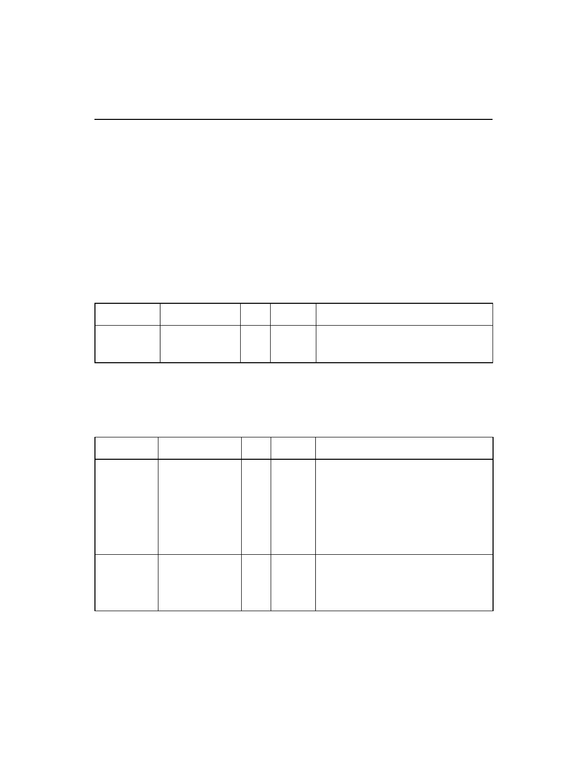
3.4 SCSI Interface Signals
The SCSI Interface signals section describes the signals for the SCSI
Channel [0] and SCSI Channel [1] interfaces.
describes the
SCSI bus clock signal that is common to both SCSI Channel [0] and
SCSI Channel [1].
In the LVD mode, the negative and positive signals form the differential
pair. In the SE mode, the negative signals represent the signal pin and
the positive signals are a virtual ground. The LSI53C1030 does not
support the HVD mode. If HVD signalling is present, the SCSI channel
3-states its drivers.
3.4.1 SCSI Channel [0] Signals
describes the SCSI Channel [0] Interface signals.
Table 3.8
SCSI Bus Clock Signal
Signal Name
BGA Position
Type
Strength
Description
SCLK
F3
I
N/A
SCSI Clock provides the 80 MHz reference
clock source for the ARM966E-S
processors and all SCSI-related timings.
Table 3.9
SCSI Channel [0] Interface Signals
Signal Name
BGA Position
Type
Strength
Description
A_SD[15:0]-
A_SD[15:0]+
Y1, AA2, AB2,
AD1, F2, G2, J4,
H1, R4, T5, T2, U2,
U5, V2, V4, W4
W5, Y2, AA3, AC1,
D1, G1, H4, H2,
P3, R5, R2, T4, U4,
U3, V5, V3
I/O
SE:
48 mA
LVD:
12 mA
SCSI Channel [0] Data signals.
A_SDP[1:0]-
A_SDP[1:0]+
W2, P4
W1, P5
I/O
SE:
48 mA
LVD:
12 mA
SCSI Channel [0] Data Parity signals.