Figure5.3 rise and fall time test condition, Rise and fall time test condition – Avago Technologies LSI53C1030 User Manual
Page 132
5-8
Specifications
Version 2.2
Copyright © 2001, 2002, 2003 by LSI Logic Corporation. All rights reserved.
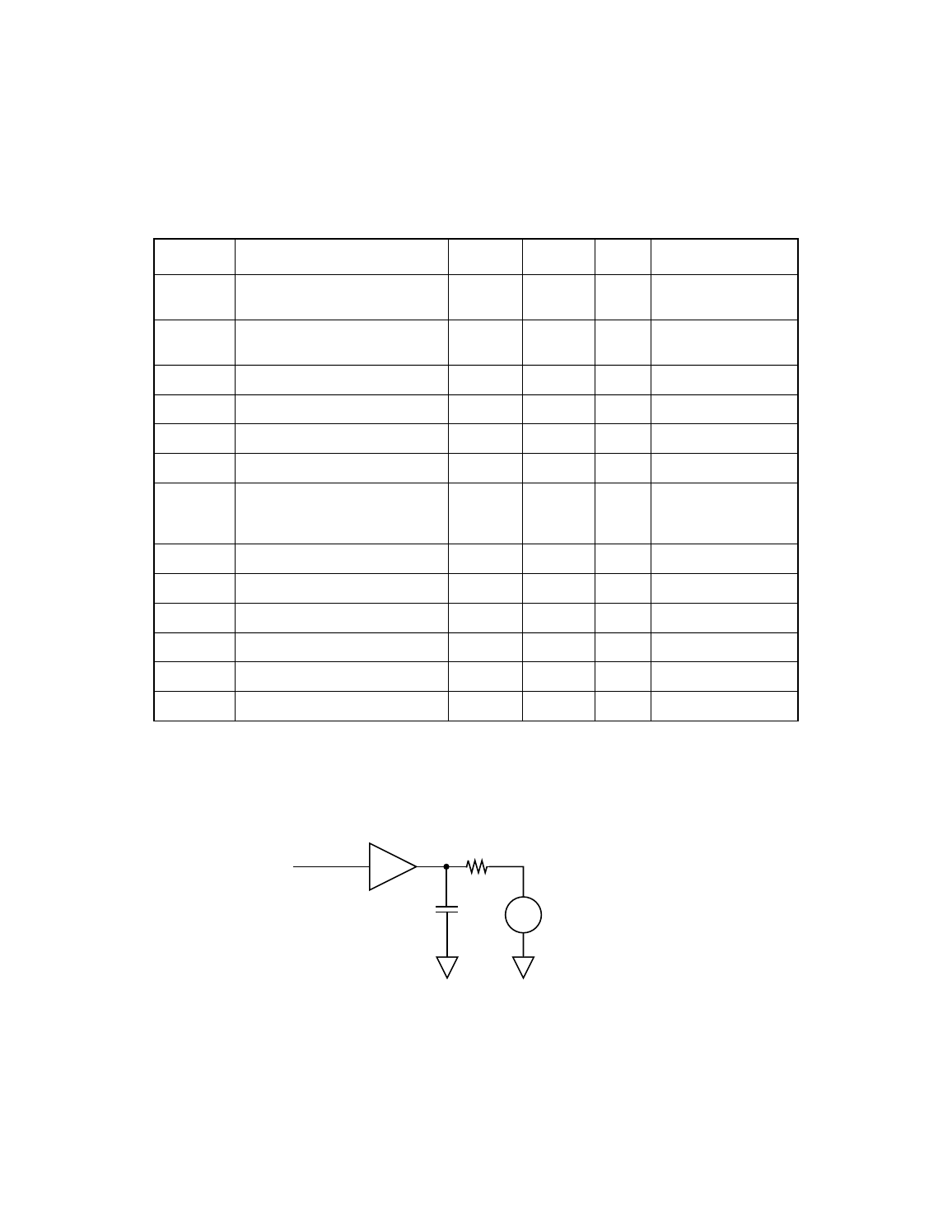
Figure 5.3
Rise and Fall Time Test Condition
I
LH
Input high leakage
–
20
µ
A
−
0.5 DD <5.25 V PIN = 2.7 V I LL Input low leakage – 20 µ A − 0.5 DD <5.25 V PIN = 0.5 V R I Input resistance 20 – M Ω Receivers disabled C P Capacitance per pin – 8 pF PQFP dV H /dt Slew rate LOW to HIGH 110 540 mV/ns dV L /dt Slew rate HIGH to LOW 110 540 mV/ns ESD HBM Electrostatic discharge (HBM) 2 – kV MIL-STD-883C; Method 3015-7; 100 pF at 1.5 k Ω ESD CDM Electrostatic discharge (CDM) 0.5 – kV ESD DS5.3.1-1996 Latch-up 100 – mA – Filter delay 20 30 ns Ultra filter delay 10 15 ns Ultra2 filter delay 5 8 ns Extended filter delay 40 60 ns 1. These values are guaranteed by periodic characterization; they are not 100% tested on every device. 2. Active negation outputs only: Data, Parity, SREQ/, and SACK/. SCSI SE mode only (minus pins). Table 5.12 TolerANT Technology Electrical Characteristics for SE SCSI 1 (Cont.) Symbol Parameter Min Max Units Test Conditions + - 2.5 V 47 Ω 20 pF
3. Single pin only; irreversible damage can occur if sustained for longer than one second.
Signals