Figure1.1 typical lsi53c1030 board application, Typical lsi53c1030 board application – Avago Technologies LSI53C1030 User Manual
Page 19
General Description
1-3
Version 2.2
Copyright © 2001, 2002, 2003 by LSI Logic Corporation. All rights reserved.
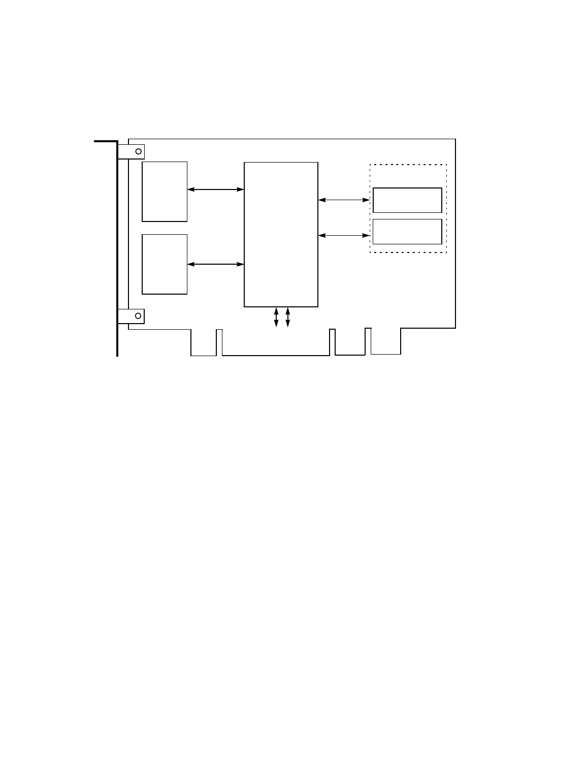
Figure 1.1
Typical LSI53C1030 Board Application
The LSI53C1030 integrates two high-performance SCSI Ultra320 cores
and a 64-bit, 133 MHz PCI-X bus master DMA core. The LSI53C1030
employs three ARM966E-S processors to meet the data transfer flexibility
requirements of the Ultra320 SCSI, PCI, and PCI-X specifications.
Separate ARM
®
processors support each SCSI channel and the
PCI/PCI-X interface.
These processors implement the LSI Logic Fusion-MPT™ architecture,
a multithreaded I/O algorithm that supports data transfers between the
host system and SCSI devices with minimal host processor intervention.
Fusion-MPT technology provides an efficient architecture that solves the
protocol overhead problems of previous intelligent and nonintelligent
adapter designs.
LVDlink™ technology is the LSI Logic implementation of Low Voltage
Differential (LVD) SCSI. LVDlink transceivers allow the LSI53C1030 to
perform either Single-Ended (SE) or LVD transfers.
illustrates
a typical LSI53C1030 system application.
Flash ROM/
Memory Control
Block
LSI53C1030
64 Bit, 133 MHz
Multifunction PCI-X
Dual Channel
Channel [0]
68 Pin
Wide SCSI
Connector
SCSI Bus
SCSI Bus
PCI-X Interface
Memory
Address/Data
Bus
Serial Data
Ultra320 SCSI
Controller
and
Terminator
Channel [1]
68 Pin
Wide SCSI
Connector
and
Terminator
Function [1]
Function [0]
Serial EEPROM
Serial Clock
NVSRAM