Figure5.4 scsi input filtering, 3 ac characteristics, Table 5.13 external clock – Avago Technologies LSI53C1030 User Manual
Page 133: Ac characteristics, Scsi input filtering, External clock, Section 5.3, “ac characteristics, Figure 5.4
AC Characteristics
5-9
Version 2.2
Copyright © 2001, 2002, 2003 by LSI Logic Corporation. All rights reserved.
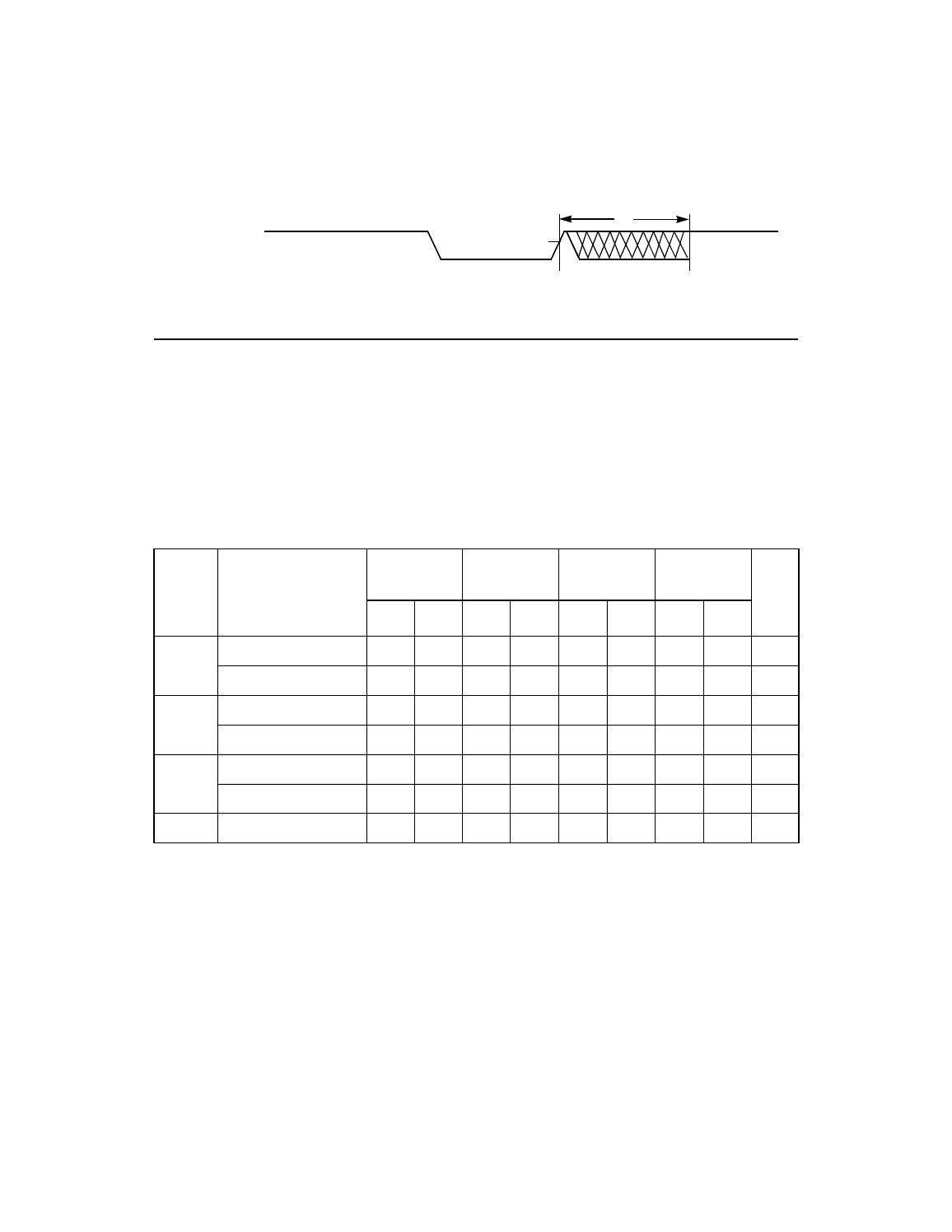
Figure 5.4
SCSI Input Filtering
5.3 AC Characteristics
The AC characteristics described in this section apply over the entire
range of operating conditions (refer to
Section 5.1, “DC Characteristics”
).
Chip timing is based on simulation at worst case voltage, temperature,
and processing. Timing was developed with a load capacitance of 50 pF.
and
provide external clock timing data.
REQ/ or ACK/ Input
t
1
V
TH
Note: t
1
is the input filtering period.
Table 5.13
External Clock
Symbol Parameter
133 MHz
PCI-X
66 MHz
PCI-X
66 MHz
PCI
33 MHz
PCI
Units
Min
Max
Min
Max
Min
Max
Min
Max
t
1
PCI Bus clock period
1
1. For frequencies above 33 MHz, the clock frequency can not be changed beyond the spread spec-
trum limits except while RST/ is asserted.
7.5
20
15
20
15
30
30
250
ns
SCSI clock period
12.5
12.5
12.5
12.5
12.5
12.5
12.5
12.5
ns
t
2
PCI CLK LOW time
2
2. Duty cycle not to exceed 60/40.
3
–
6
–
6
–
11
–
ns
SCLK LOW time
5
7.5
5
7.5
5
7.5
5
7.5
ns
t
3
PCI CLK HIGH time
3
–
6
–
6
–
11
–
ns
SCLK HIGH time
5
7.5
5
7.5
5
7.5
5
7.5
ns
t
4
PCI CLK slew rate
1.5
4
1.5
4
1.5
4
1
4
V/ns