Avago Technologies LSI53C1030 User Manual
Page 71
SCSI Interface Signals
3-11
Version 2.2
Copyright © 2001, 2002, 2003 by LSI Logic Corporation. All rights reserved.
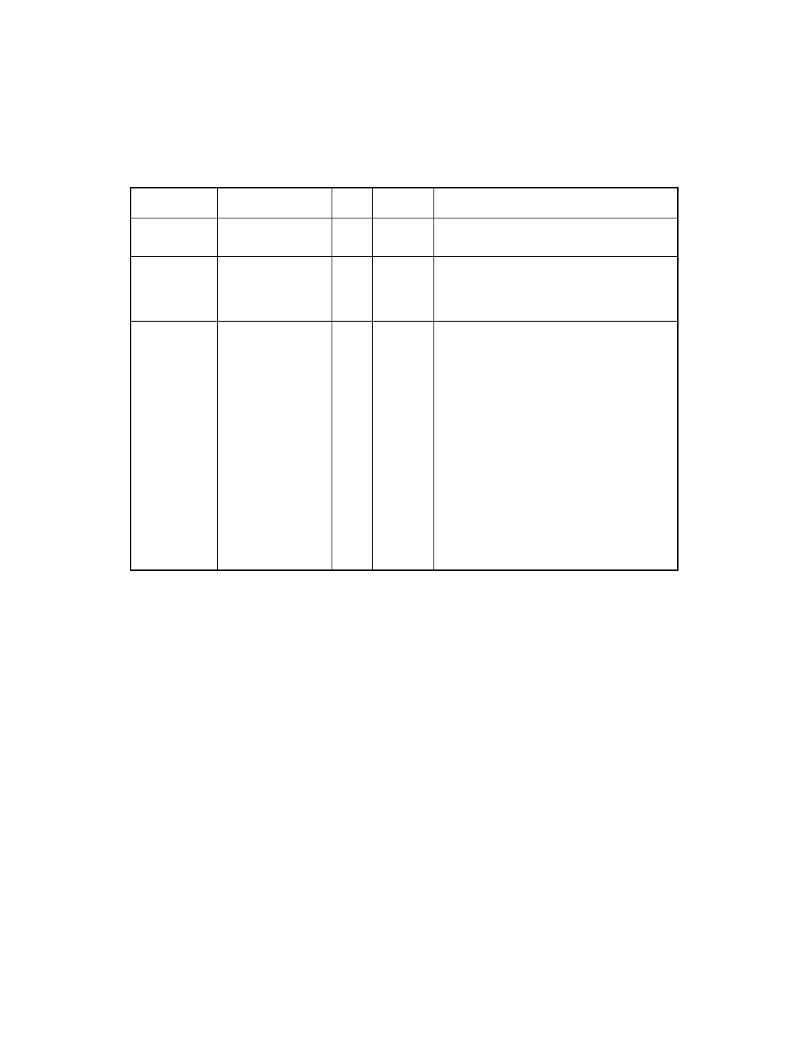
A_VDDBIAS
T1
O
N/A
A_VDDBIAS provides power for the
A_RBIAS circuit.
A_RBIAS
R1
I
N/A
Connect a 9.76 k
Ω
or 10.0 k
Ω
resistor
between the A_VDDBIAS and A_RBIAS
pins to generate the LVD signalling pad bias
current.
A_DIFFSENS
E2
I
N/A
The SCSI Channel [0] Differential Sense
pin detects the present mode of the SCSI
bus. This signal is 5 V tolerant and must
connect to the DIFFSENS signal on the
physical SCSI bus.
SE Mode: Driving this pin below 0.5 V
(LOW) indicates an SE bus and places
SCSI Channel [0] in the SE bus mode.
LVD Mode: Driving this signal between 0.7 V
and 1.9 V (intermediate) indicates an LVD
mode and places SCSI Channel [0] in the
LVD bus mode.
HVD Mode: Driving this pin above 2.0 V
(HIGH) indicates an HVD bus and causes
SCSI Channel [0] to 3-state its SCSI drivers.
Table 3.9
SCSI Channel [0] Interface Signals (Cont.)
Signal Name
BGA Position
Type
Strength
Description
- MGA-725M4 (4 pages)
- MGA-71543 (4 pages)
- MGA-71543 (3 pages)
- MGA-82563 (6 pages)
- 3ware 9690SA-8I (Channel) (380 pages)
- 3ware SAS 9750-8i (48 pages)
- 3ware 9690SA-8I (Channel) (138 pages)
- 3ware 9550SXU-8LP (Channel) (149 pages)
- 3ware SAS 9750-8i (29 pages)
- 3ware 9550SXU-8LP (Channel) (40 pages)
- 3ware 9650SE-8LPML (Channel) (45 pages)
- 3ware 9690SA-8I (Channel) (27 pages)
- 3ware 9690SA-8I (Channel) (361 pages)
- 6160 SAS Switch (2 pages)
- Cache Protection for RAID Controller Cards (13 pages)
- MegaRAID SAS 9271-8iCC (13 pages)
- MegaRAID SAS 9361-8i (13 pages)
- MegaRAID SAS 9266-8i (12 pages)
- MegaRAID SAS 9380-8e (43 pages)
- Cache Protection for RAID Controller Cards (139 pages)
- MegaRAID SAS 9285-8ecv (80 pages)
- MegaRAID SAS 9285-8ecv (92 pages)
- MegaRAID SAS 9266-8i (20 pages)
- MegaRAID SAS 9271-8iCC (26 pages)
- MegaRAID SafeStore Software (502 pages)
- MegaRAID SAS 0260CV-4i (72 pages)
- MegaRAID SAS 0260CV-4i (64 pages)
- MegaRAID SAS 0260CV-4i (49 pages)
- MegaRAID SAS 9271-8i (8 pages)
- MegaRAID SAS 9361-8i (7 pages)
- MegaRAID SAS 9341-8i (8 pages)
- MegaRAID SAS 9380-4i4e (7 pages)
- MegaRAID SAS 9380-8e (7 pages)
- MegaRAID SAS 0260CV-4i (28 pages)
- MegaRAID SAS 9240-8i (4 pages)
- MegaRAID SAS 9280-24i4e (16 pages)
- MegaRAID SAS 9260-16i (12 pages)
- MegaRAID SAS 9280-24i4e (14 pages)
- MegaRAID SAS 9260-8i (4 pages)
- MegaRAID SafeStore Software (8 pages)
- MegaRAID SAS 9280-8e (22 pages)
- MegaRAID SAS 9261-8i (4 pages)
- MegaRAID SAS 9285-8e (12 pages)
- MegaRAID SAS 9280-16i4e (12 pages)
- MegaRAID SAS 9280-4i4e (4 pages)