Interrupt pin, Minimum grant, Register: 0x3d – Avago Technologies LSI53C1030 User Manual
Page 102: Register: 0x3e
4-16
PCI Host Register Description
Version 2.2
Copyright © 2001, 2002, 2003 by LSI Logic Corporation. All rights reserved.
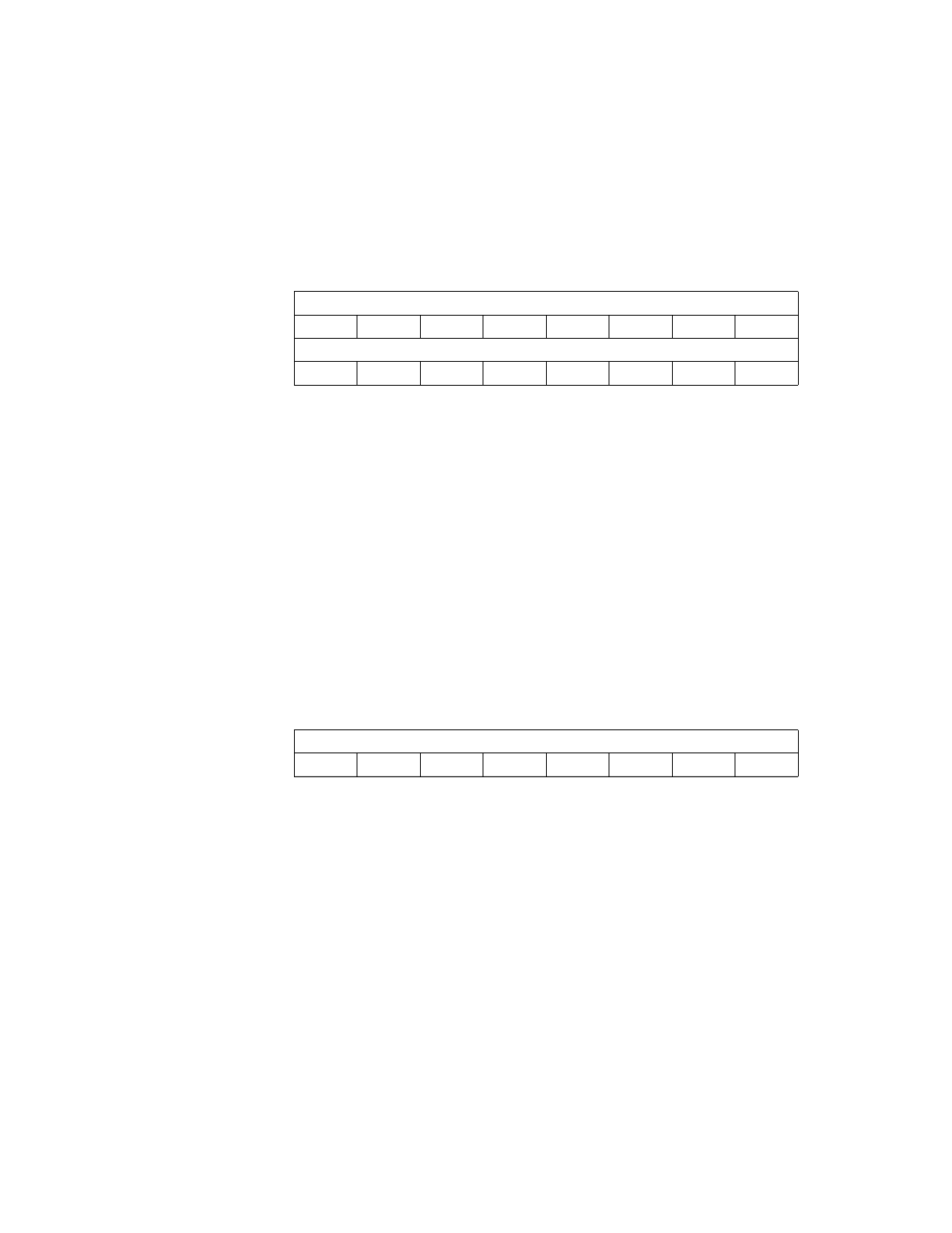
Register: 0x3D
Interrupt Pin
Read Only
Interrupt Pin
[7:0]
The encoding of this read only register is unique to each
function on the LSI53C1030. It indicates which interrupt
pin the function uses. The value for Function [0] is 0x01,
which indicates that Function [0] presents interrupts on
the INTA/ or ALT_INTA pins. The value for Function [1] is
0x02, which indicates that Function [1] presents inter-
rupts on the INTB/ or ALT_INTB/ pins. The Interrupt
Request Routing Mode bits, bits [9:8] in the
register, determine if the function presents inter-
rupts on INTx/, ALT_INTx/, or both.
Register: 0x3E
Minimum Grant
Read Only
Min_Gnt
[7:0]
This register specifies the desired settings for the latency
timer values in units of 0.25
µ
s. This register specifies
how long of a burst period the device needs. The
LSI53C1030 sets this register to 0x10, indicating a burst
period of 4.0
µ
s.
7
0
Function [0] Interrupt Pin
0
0
0
0
0
0
0
1
Function [1] Interrupt Pin
0
0
0
0
0
0
1
0
7
0
Minimum Grant
0
0
0
1
0
0
0
0